Submount for light emitting/receiving device

a light-emitting/receiving device and sub-mount technology, which is applied in the direction of semiconductor laser structure details, optical resonator shape and construction, semiconductor lasers, etc., can solve the problems of poor heat dissipation of light-emitting devices, difficult to obtain excellent reflecting surfaces, and high cost of sub-mounts, etc., to achieve excellent light transmission performance, easy formation of reflecting surfaces parallel, and high efficiency

Inactive Publication Date: 2007-05-31
SHARP KK
View PDF8 Cites 17 Cited by
  • Summary
  • Abstract
  • Description
  • Claims
  • Application Information

AI Technical Summary

Benefits of technology

[0053] According to the method for manufacturing a submount for a light emitting / receiving device in the present invention, which includes a step of etching from a face of the substrate opposite to the mounting surface to form an outer opening and a through hole adjoining the outer opening by performing, and a step of removing the mounting surface portion of the substrate to form a device-side opening adjoining the through hole and having a specified size, it becomes implementable to adjust the size of the device-side opening easily and with high efficiency.
[0051] According to this embodiment, the size of the device-side opening can be adjusted easily by removing the portion of the substrate corresponding to the mounting surface by polishing.
[0052] As described above, the submount for the light emitting / receiving device according to the invention is so constructed that the reflecting surface is formed parallel with a specified crystal orientation face, where the reflecting surface continue into the device-side opening provided in the mounting surface for the light emitting / receiving device to be mounted, and the outer opening provided in the face opposite to the mounting surface. Therefore, light inputted to or outputted from the light emitting / receiving device can be reflected with high efficiency. By crystal anisotropic etching for example, it is possible to easily form the reflecting surface parallel with the crystal orientation face. Thus, it is possible to easily form a submount for a light emitting / receiving device having excellent light transmission performance.
[0053] According to the method for manufacturing a submount for a light emitting / receiving device in the present invention, which includes a step of etching from a face of the substrate opposite to the mounting surface to form an outer opening and a through hole adjoining the outer opening by performing, and a step of removing the mounting surface portion of the substrate to form a device-side opening adjoining the through hole and having a specified size, it becomes implementable to adjust the size of the device-side opening easily and with high efficiency.

Problems solved by technology

However, there would be a problem of poor heat dissipation in the light-emitting device 102 when the light guide member 103 is made of a light-pervious material such as glass or light-pervious resin for enhancement of the light transmission performance.
There is also a problem that the submount becomes expensive since the light-pervious material is higher in price than Si material or the like.
In the case where the light guide member 103 is formed from a metal material by metal stamping at low cost, there can be a problem that it is difficult to obtain an excellent reflecting surface, that is, excellent light transmission performance since the surface of the through hole is liable to flaws.

Method used


Image

  • Submount for light emitting/receiving device
  • Submount for light emitting/receiving device
  • Submount for light emitting/receiving device

Examples


Embodiment Construction

[0084] Hereinbelow, the present invention will be described in detail by way of embodiments thereof illustrated in the accompanying drawings.

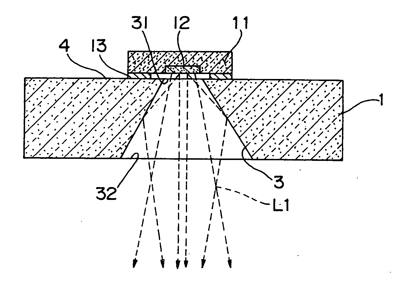
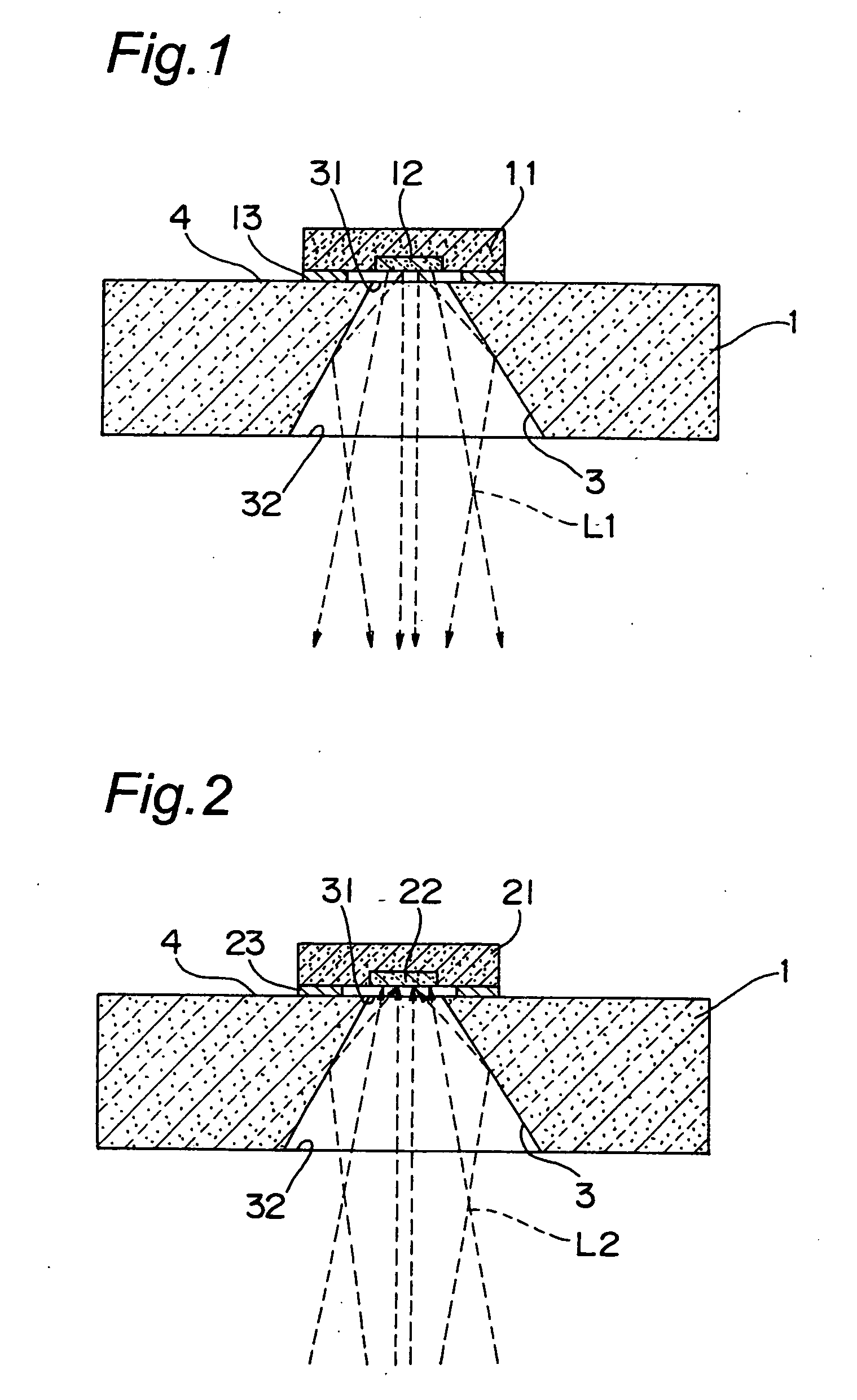
[0085]FIG. 1 is a schematic sectional view showing a submount for a light-emitting device according to an embodiment of the present invention.

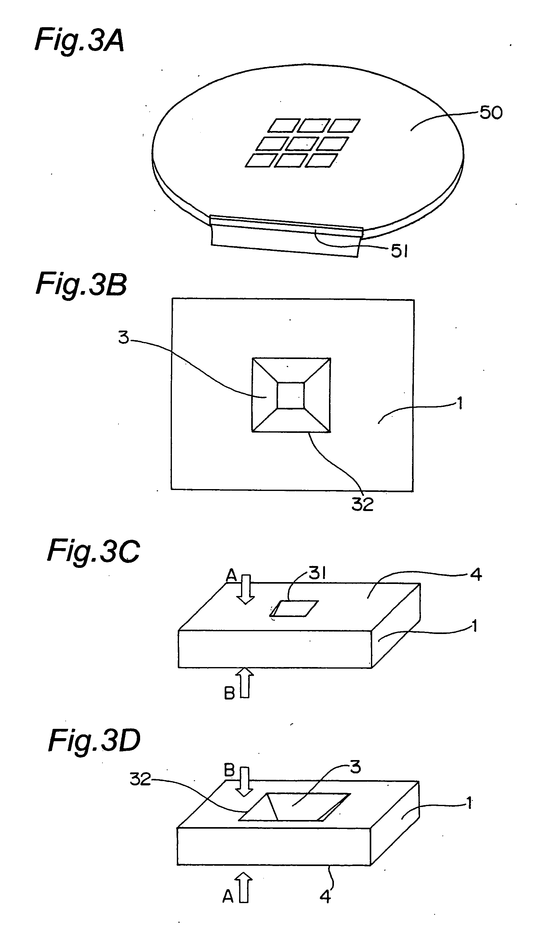
[0086] This submount for a light-emitting device includes a submount main body 1, a through hole 3 formed in the submount main body 1 by anisotropic etching, a device-side opening 31 formed in a light-emitting device mounting surface 4 of the submount main body and adjoining the through hole 3, and an outer opening 32 formed in an outer side face opposed to the light-emitting device mounting surface 4 of the submount main body 1. On the light-emitting device mounting surface 4 of the submount, a light-emitting device 11 is mounted via an electrode 13, so that a light-emitting portion 12 of this light-emitting device faces the device-side opening 31. That is, the light-emitting device 11 is electrically ...


PUM


Abstract

In a submount main body (1) composed of a single crystal silicon, a mounting surface (4) on which a light-emitting device (11) is mounted is composed of a (100)-oriented surface and the inner surface of a through hole (3) which is formed by anisotropic etching is parallel to the (110)-oriented surface. The light-emitting portion of the light-emitting device (11) is arranged to face a device-side opening (31) which opens into the mounting surface (4) of the submount main body (1). Consequently, heat generated in the light-emitting device (11) can be discharged to the outside more efficiently than the case where the light-emitting portion is arranged to face a side opposite to the submount side. Specifically, light from the light-emitting device (11) is reflected by a reflective surface formed on the surface of the through hole (3), and highly efficiently transmitted outside of the submount main body (1).

Description

TECHNICAL FIELD [0001] The present invention relates to a submount for a light emitting / receiving device which is used for, for example, optical communications, automobiles and the like and which requires reduction of power consumption and performance of heat dissipation. BACKGROUND ART [0002] In recent years, together with the progress toward higher brightness of LEDs (Light Emitting Diodes), there has been an increasing demand for higher heat dissipation to the submount on which those LEDs are mounted. As an example of the submount of high heat dissipation, a submount using diamond is cited. The submount of diamond is used in optical communication systems for long distance transmission. Optical communication systems for long distance transmission, because of their relatively high prices, permit the use of higher-cost component parts such as diamond. [0003] However, low-priced submounts are indispensable for cost reduction in the illumination or on-vehicle equipment using plural hi...

Claims


Application Information

Patent Timeline
Patent Type & Authority Applications(United States)
IPC IPC(8): H01S3/08H01L31/02H01L31/0203H01L31/0232H01L33/44H01L33/60H01L33/62H01L33/64H01S5/00H01S5/02
CPCH01L31/0203H01L31/0232H01L33/60H01L2924/0002H01L2924/00H01L31/02327
Inventor ISHII, YORISHIGE
Owner SHARP KK
Why Eureka
Try Eureka