Oxide etch with nh4-nf3 chemistry

a technology of nh4-nf3 and etching method, which is applied in the direction of electrical equipment, semiconductor devices, semiconductor/solid-state device testing/measurement, etc., can solve the problems of native oxide contamination during etching, difficulty in processing, and undesirable native oxides

Inactive Publication Date: 2007-05-31
APPLIED MATERIALS INC
View PDF28 Cites 278 Cited by
  • Summary
  • Abstract
  • Description
  • Claims
  • Application Information

AI Technical Summary

Benefits of technology

[0016] Another embodiment of the present invention provides a method for processing a substrate having an oxide structure comprising a first oxide and a second oxide comprising positioning the substrate in a vacuum chamber, cooling the substrate to a first temperature, introducing an etching gas mixture into the vacuum chamber, wherein the etching gas mixture is adjusted to reduce the first oxide at a first rate and the second oxide at a second rate, generating a plasma of the etching gas mixture within the vacuum chamber, exposing the oxide structure to the plasma to form a film on the structure, heating the substrate to vaporiz

Problems solved by technology

Native oxides may also result from contamination during etching.
Native oxides are typically undesirable and need to be removed prior to a subsequent process.
Some oxide features may have two or more oxides that respond differently to the same process, hence posing difficulties in processing, especially when feature sizes are smaller.
However, sputter etching process generally cannot completely remove oxides and can damage d

Method used


Image

  • Oxide etch with nh4-nf3 chemistry
  • Oxide etch with nh4-nf3 chemistry
  • Oxide etch with nh4-nf3 chemistry

Examples


example

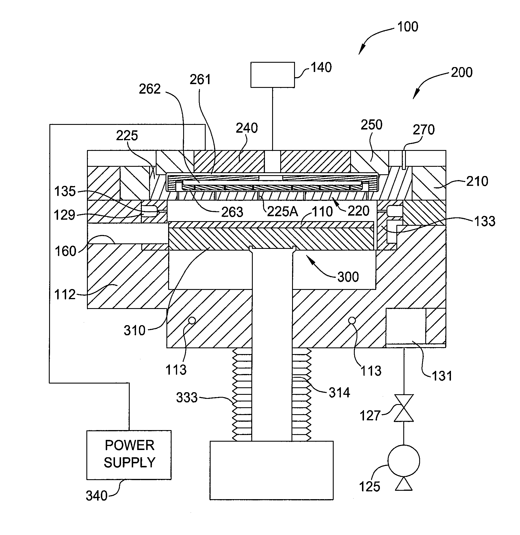
[0079] During etching, a gas mixture of 2 sccm of NF3, 10 sccm of NH3 and 2,500 sccm of argon was introduced into a vacuum chamber, such as the processing chamber 100. A plasma of the gas mixture was ignited using 100 Watts of power. The bottom purge was 1,500 sccm of argon and the edge purge was 50 sccm of argon. The chamber pressure was maintained at about 6 Torr, and the substrate temperature was about 22° C. The substrate was etched for 120 seconds.

[0080] During anneal, the spacing was 750 mil and the lid temperature was 120° C. The substrate was annealed for about 60 seconds. About 50 angstroms of material was removed from the substrate surface. No anneal effect was observed. The etch rate was about 0.46 angstroms per second (28 Å / min). The observed etch uniformity was about 5% for the 50 Å etch.

[0081] Unless otherwise indicated, all numbers expressing quantities of ingredients, properties, reaction conditions, and so forth, used in the specification and claims are to be unde...


PUM


Abstract

The present invention generally provides apparatus and methods for selectively removing various oxides on a semiconductor substrate. One embodiment of the invention provides a method for selectively removing an oxide on a substrate at a desired removal rate using an etching gas mixture. The etching gas mixture comprises a first gas and a second gas, and a ratio of the first gas and a second gas is determined by the desired removal rate.

Description

CROSS-REFERENCE TO RELATED APPLICATIONS [0001] This application is a continuation-in-part of co-pending U.S. patent application Ser. No. 11 / 137,609 (Attorney Docket No. 8802 D1), filed May 24, 2005, which is a divisional application of U.S. patent application Ser. No. 11 / 063,645 (Attorney Docket No. 8802), filed Feb. 22, 2005, which claims benefit of U.S. provisional patent application Ser. No. 60 / 547,839, filed Feb. 26, 2004. Each of the aforementioned related patent applications is herein incorporated by reference.BACKGROUND OF THE INVENTION [0002] 1. Field of the Invention [0003] Embodiments of the present invention generally relate to methods and apparatus for processing semiconductor substrates. More particularly, embodiments of the present invention relates to methods and apparatus for selective oxide etching in semiconductor fabrication. [0004] 2. Description of the Related Art [0005] In semiconductor fabrication, oxide fabrication is critical, especially for the thin oxide w...

Claims


Application Information

Patent Timeline
IPC IPC(8): H01L21/461H01L21/302
CPCH01L21/02057H01L21/02068H01L21/31055H01L21/31116H01L21/67069H01L21/76224H01L22/20H01L29/665H01L29/6656H01L29/78H01L21/3065
Inventor ARGHAVANI, REZAKAO, CHIEN-TEHLU, XINLIANG
Owner APPLIED MATERIALS INC
Why Eureka
Try Eureka