[0016] It is another aspect of the present invention to provide a method of manufacturing a printed wiring board which can ensure accuracy of a circuit pattern.
[0017] It is still another aspect of the present invention to provide a method of manufacturing a printed wiring board capable of reducing an influence of deformation that is exerted on a via conductor.
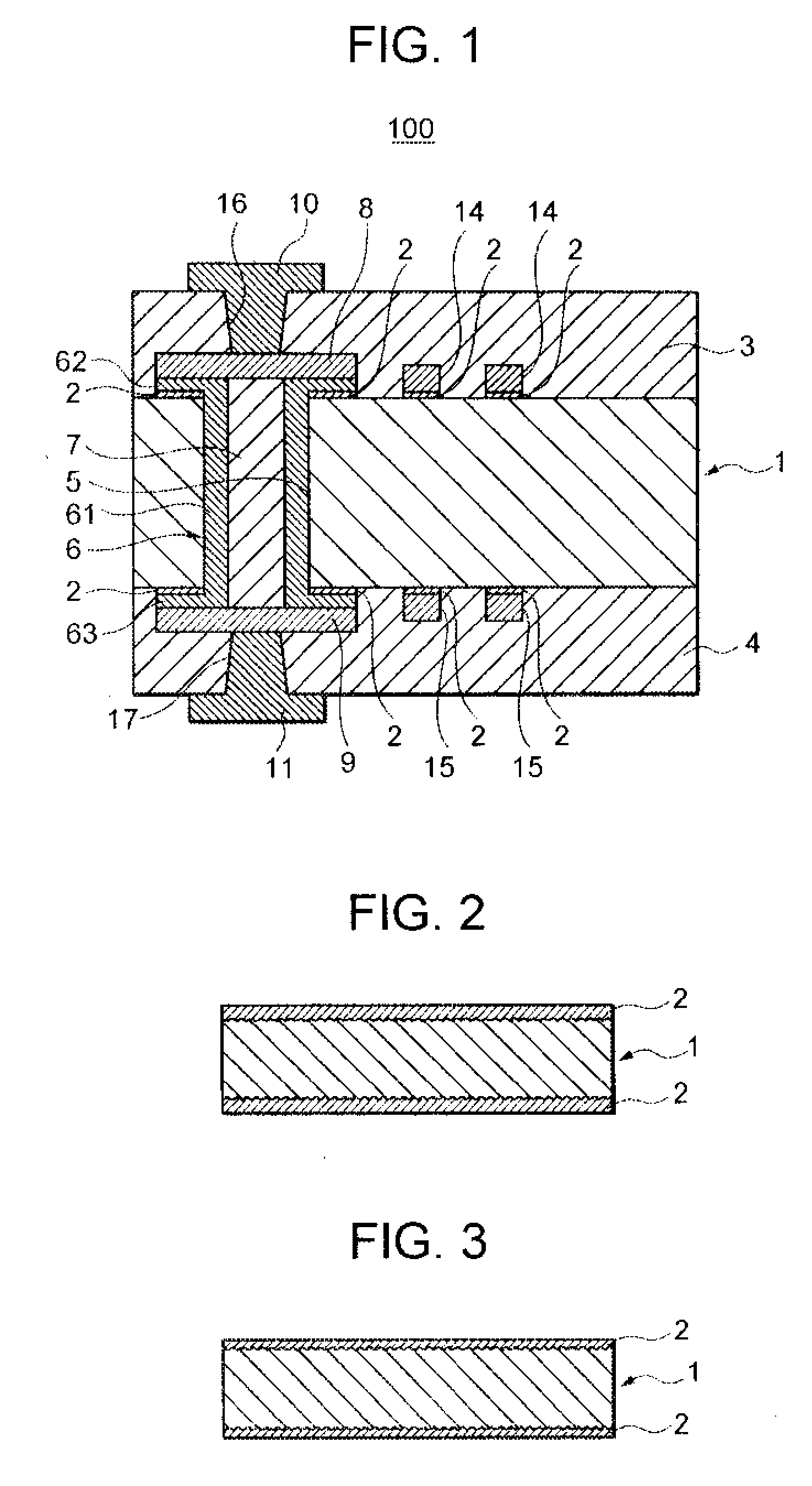
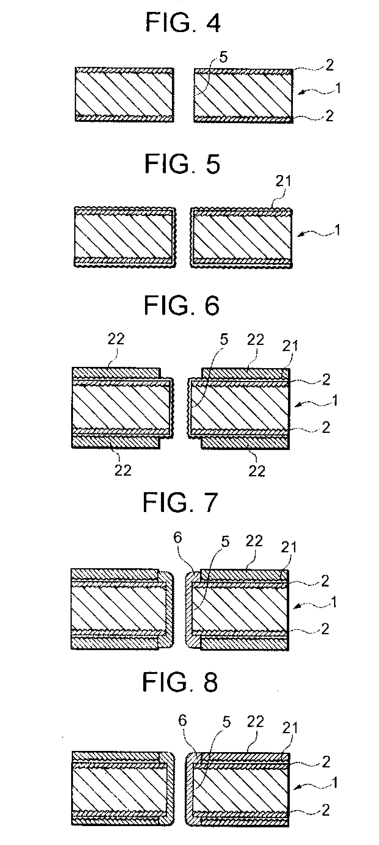
[0019] Conventionally, when a through hole where a through hole conductor is formed is filled with a resin using the screen printing method, part of the resin forms over the through hole where the through hole conductor is formed, and therefore, the part of the resin formed over the through hole (namely, an unnecessary insulating material) needs to be abraded away. In the printed wiring board according to the present invention, the positive photosensitive resin is used as a resin filled inside the through hole where the through hole conductor is formed. Therefore, an unnecessary part of the positive photosensitive resin can be easily removed by filling the through hole where the through hole conductor is formed with the positive photosensitive resin and forming the positive photosensitive resin on the opening of the through hole where the through hole conductor is formed and on the surface of the base substrate at least in the vicinity of the opening by the use of the screen printing method, and exposing and developing the positive photosensitive resin. Therefore, the abrading process can be omitted. Consequently, a circuit pattern can be formed by the additive method that conventionally could not be used due to the necessity of the abrading process. Furthermore, conventionally, when a through hole where a through hole conductor is formed is filled with a resin using the lamination method, a resin layer is also formed on the base substrate, thereby disabling formation of a capped conductor (plating) on the through hole conductor. In the printed wiring board according to the present invention, although a positive photosensitive resin layer is formed so as to cover the through hole conductor using the lamination method, an unnecessary part of the positive photosensitive resin layer covering the through hole conductor can be easily removed by the
exposure and development. Therefore, it is also possible to select the lamination method as a method of filling the through hole where the through hole conductor is formed with the resin. Accordingly, in the printed wiring board according to the present invention, the through hole where the through hole conductor is formed can be filled with the resin by either the screen printing method or the lamination method, and the circuit pattern can be formed either by the subtractive method or the additive method. Incidentally, if the circuit pattern is formed by the additive method, the accuracy of its shape can be ensured.
[0021] In this event, the part of the positive photosensitive resin formed over the through hole where the through hole conductor is formed is exposed to the light by the initial
exposure. Then, the
exposure is carried out using the
photomask that shields the opening of the through hole from the light. As a result, the unnecessary part of the positive photosensitive resin is exposed so as to be easily removed.
[0023] Conventionally, when forming the through hole conductor by plating, a plating layer that becomes part of the circuit pattern is also formed on the base substrate, and therefore, the circuit pattern is relatively thick. On the other hand, in the present invention, when forming the through hole conductor by plating, the
resist is formed on the base substrate so that the plating layer that becomes part of the circuit pattern is not formed on the base substrate. The circuit pattern is formed in a subsequent step. Therefore, the circuit pattern can be formed to be thinner than the circuit pattern produced by the conventional method. Accordingly, even if the circuit pattern is formed by the subtractive method, the accuracy of its shape can be ensured and the formation of a fine circuit pattern is made possible.
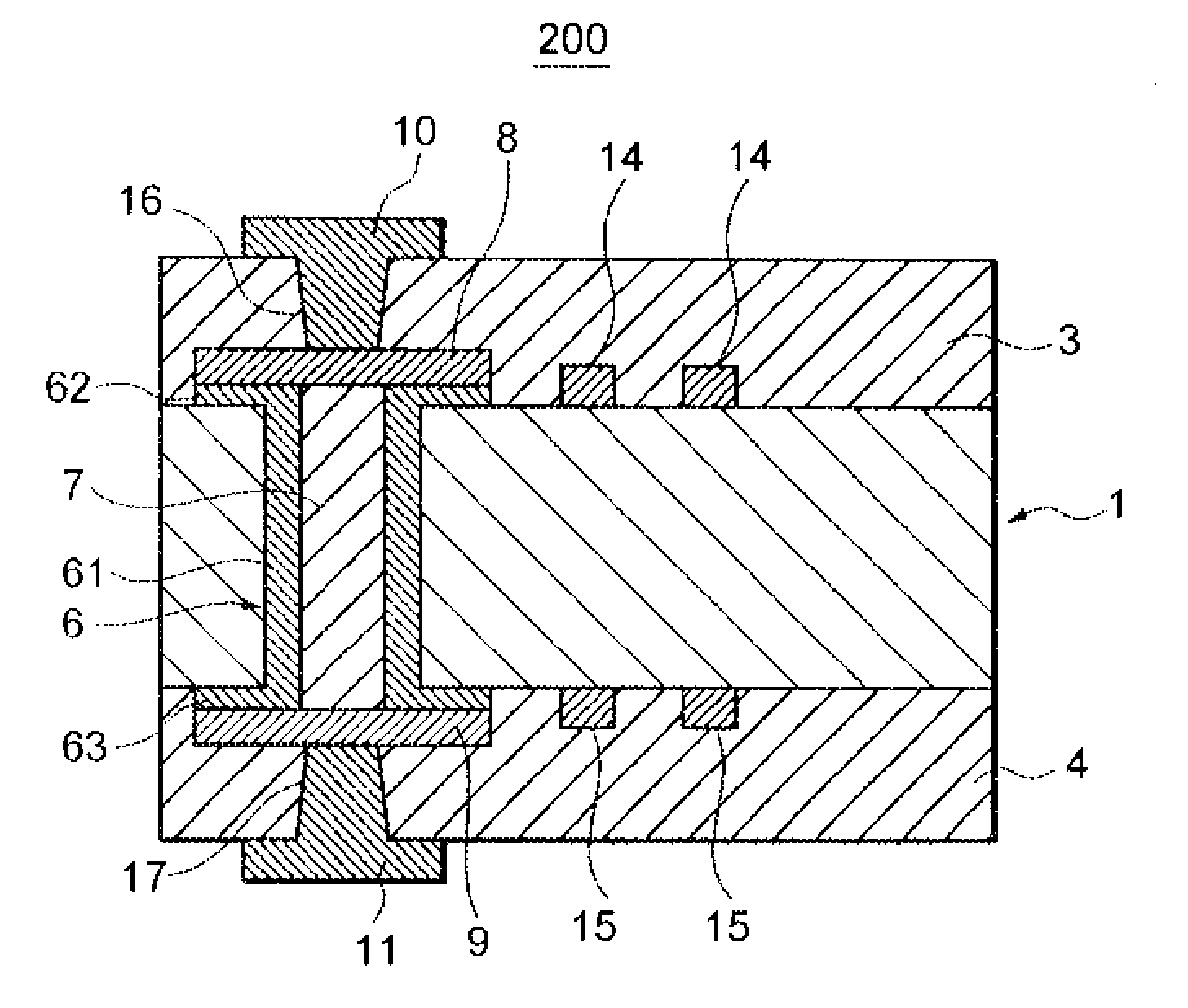
[0027] Further, inasmuch as the conventional circuit pattern includes the first and second conductors, the first and second conductors should be reduced in thickness for forming a thin circuit pattern. Therefore, the capped conductor being the same layer as the second conductor should also be formed thin. In the manufacturing method for the printed wiring board according to the present invention, the circuit pattern does not include the first conductor. Accordingly, even if the second conductor is formed thicker compared to the conventional second conductor, the circuit pattern of the present invention can still be formed thinner than the conventional circuit pattern. To this end, the capped conductor of the present invention can be formed thicker than the conventional capped conductor. In the printed wiring board, deformation is caused by differences in the
thermal expansion coefficients among the through hole conductor, the resin filled inside the through hole where the through hole conductor is formed, and the base substrate. However, by increasing the thickness of the capped conductor, an influence of the deformation exerted on the via conductor can be relaxed.

