Method of direct plating of copper on a substrate structure

a substrate structure and copper technology, applied in the direction of semiconductor devices, semiconductor/solid-state device details, electrical equipment, etc., can solve the problems of insufficient support of future interconnect technology, void-free filling of interconnect features via conventional metallization techniques, and difficult to have adequate seed step coverage with pvd techniques,

Inactive Publication Date: 2007-06-07
APPLIED MATERIALS INC
View PDF34 Cites 47 Cited by
  • Summary
  • Abstract
  • Description
  • Claims
  • Application Information

AI Technical Summary

Benefits of technology

[0012] The present invention teaches a method for depositing a copper seed layer onto a substrate surface, generally onto a barrier layer or an adhesion layer. The barrier or adhesion layer may include a refractory metal and/or a group VIII metal. The method includes cathodically pre-treating the substrate surface in an acid-containing solution that is free of copper ions. The substrate is then placed into a neutral or alkaline (pH≧7.0) copper solution that includes complexed copper ions and a current or bias is applied across the substrate surface. The complexed copper ions include a carboxylate ligand, such as oxalate or tartrate, or ethylenediamine (ED), EDTA and/or acetate. The complexed...

Problems solved by technology

However, as interconnect sizes decrease and aspect ratios of device features increase, void-free filling of interconnect features via conventional metallization techniques becomes increasingly difficult.
As a result thereof, conventional plating processes will likely be inadequate to support the demands of future interconnect technologies.
However, it is extremely difficult to have adequate seed step coverage with PVD techniques, as discontinuous islands of copper agglomerates are often obtained close to the feature bottom in high aspect ratio features with PVD techniques.
For PVD techniques, a thick copper layer (e.g., >200 Å) over the field is generally needed to have continuous sidewall coverage throughout the depth of the features, which often causes the throat of the feature to close before the feature sidewalls are covered.
For CVD processes, copper purity is generally q...

Method used


Image

  • Method of direct plating of copper on a substrate structure
  • Method of direct plating of copper on a substrate structure
  • Method of direct plating of copper on a substrate structure

Examples


Embodiment Construction

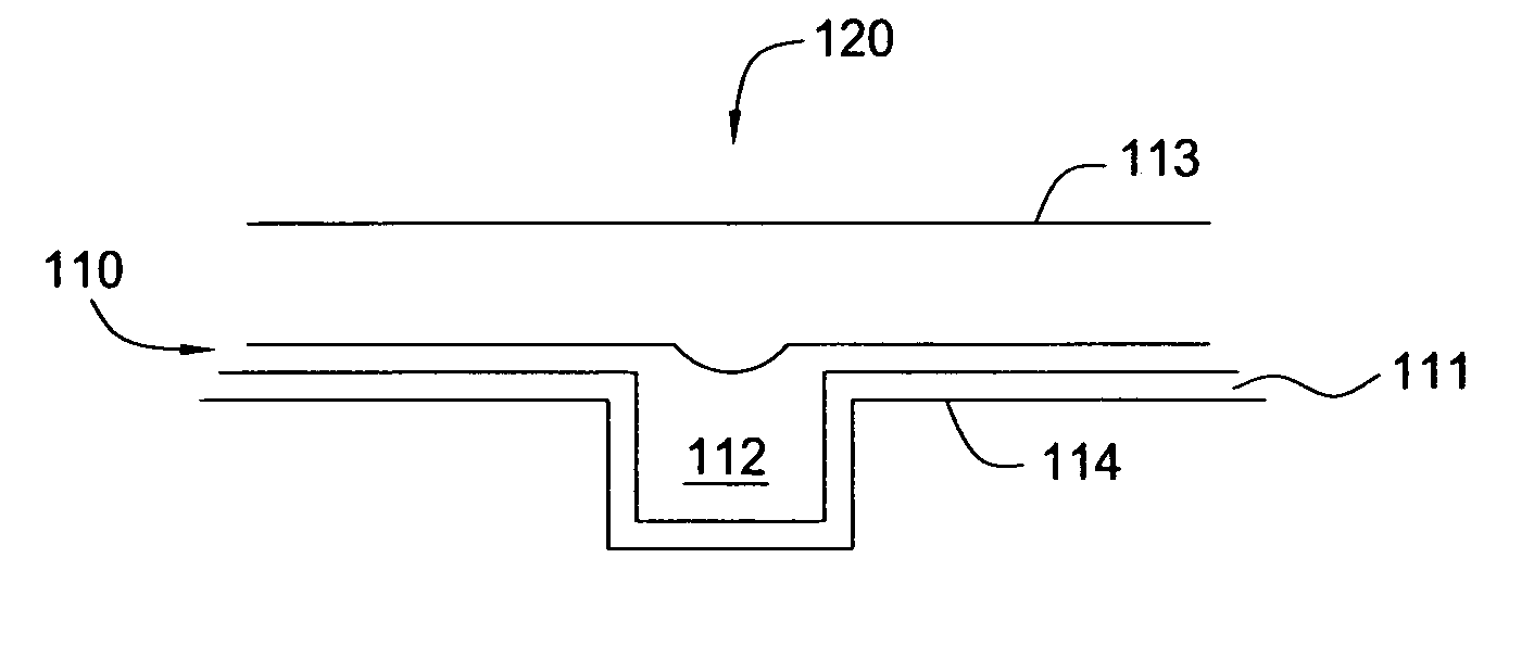
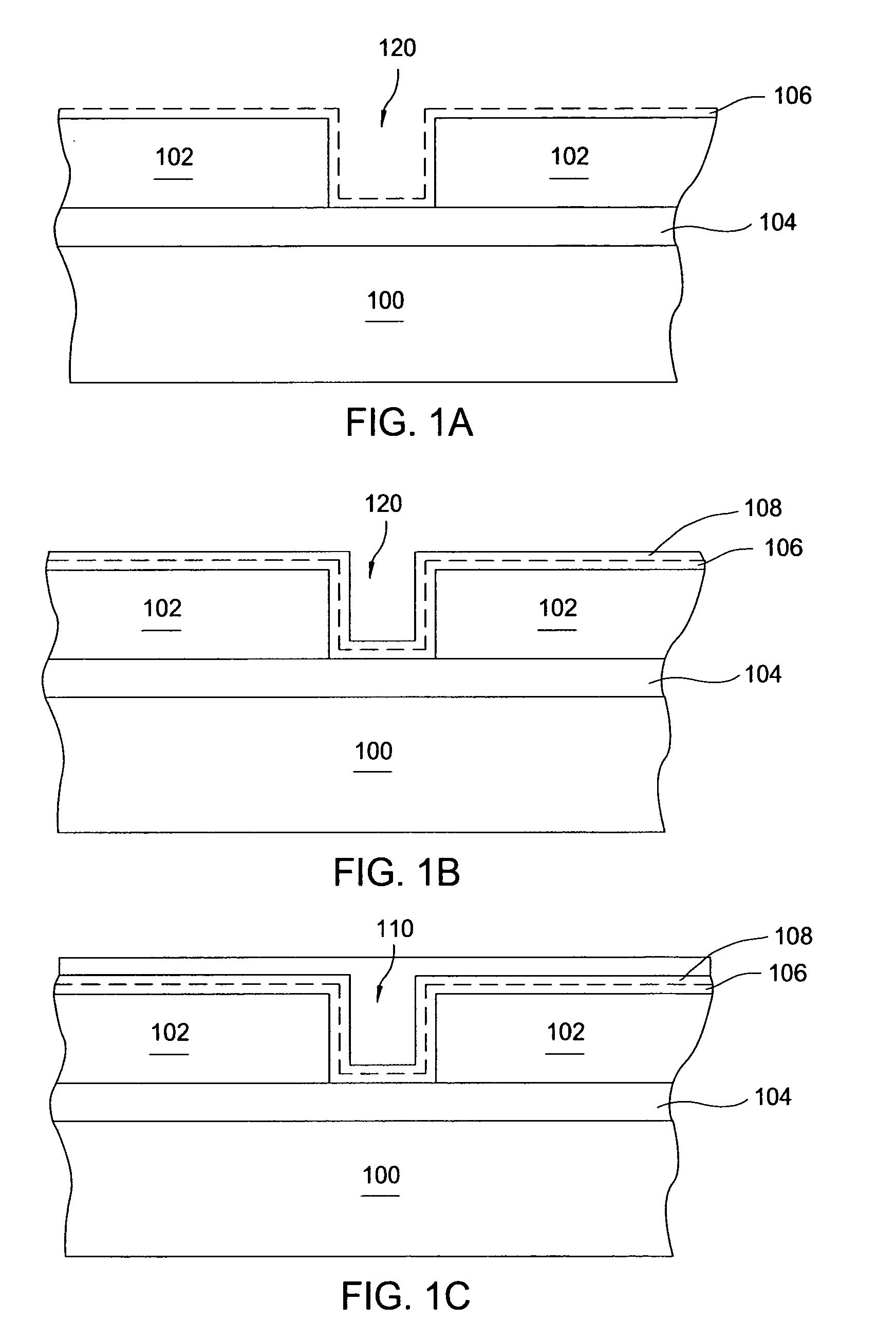
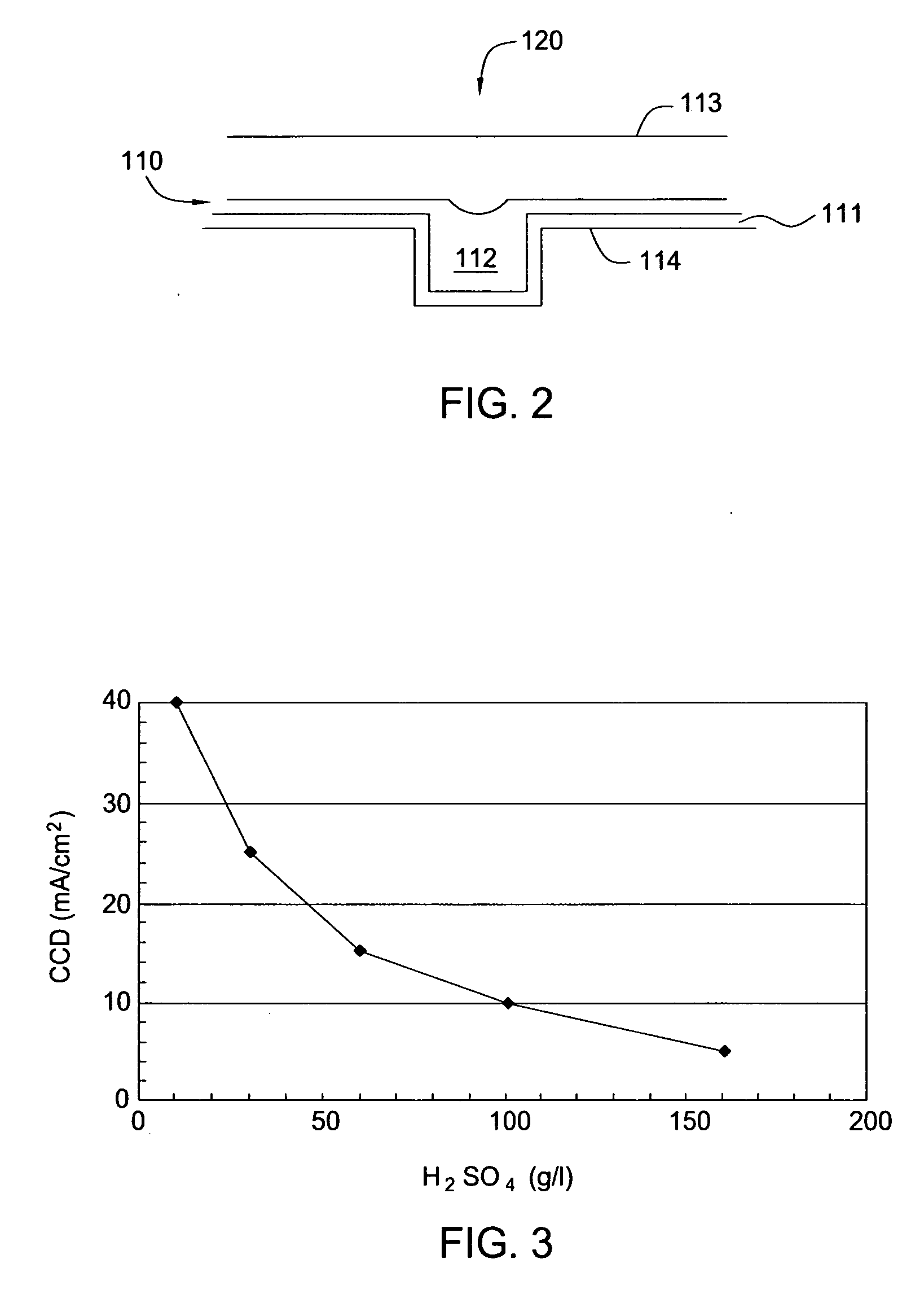
[0021] The present invention teaches a method for depositing a copper layer onto a substrate surface, generally onto a barrier or adhesion layer. The barrier layer may include a refractory metal and / or a group VIII metal. The term group VIII metals (e.g., old CAS system notation) is generally intended to describe group 8, 9 and 10 elements, such as ruthenium (Ru), rhodium (Rh), palladium (Pd), cobalt (Co), nickel (Ni), osmium (Os), iridium (Ir), and platinum (Pt). The method includes cathodically pre-treating the substrate surface in an acid-containing solution that is free of copper ions. This pre-treatment reduces the critical current density (CCD) required for forming a continuous and void-free seed layer on the barrier or adhesion layer via an ECP process. The substrate is then placed into a neutral or alkaline (pH≧7.0) complex copper solution that includes complexed copper ions and a current or bias is applied across the substrate surface. A “complex bath” or “complex solution”...


PUM

PropertyMeasurementUnit
Concentrationaaaaaaaaaa
Percent by atomaaaaaaaaaa

Abstract

The present invention teaches a method for depositing a copper seed layer onto a substrate surface, generally onto a barrier layer. The barrier layer may include a refractory metal and/or a group 8, 9 or 10 metal. The method includes cathodically pre-treating the substrate in an acid-containing solution. The substrate is then placed into a copper solution (pH≧7.0) that includes complexed copper ions and a current or bias is applied across the substrate surface. The complexed copper ions are reduced to deposit a copper seed layer onto the barrier layer. In one aspect, a complex alkaline bath is then used to electrochemically plate a gapfill layer on the substrate surface, followed by overfill in the same bath. In another aspect, an acidic bath ECP gapfill process and overfill process follow the alkaline seed layer process.

Description

CROSS-REFERENCE TO RELATED APPLICATIONS [0001] This application claims benefit of U.S. provisional patent application Ser. No. 60 / 621,173 [APPM 9762L], filed Oct. 21, 2004, which is herein incorporated by reference. [0002] This application is a continuation-in-part of co-pending U.S. patent application Ser. No. 11 / 007,857 [APPM 9200], filed Dec. 9, 2004, which claims benefit of U.S. Provisional Patent Application Ser. No. 60 / 579,129, filed Jun. 10, 2004. This application is also a continuation-in-part of co-pending U.S. patent application Ser. No. 11 / 012,965 [APPM 9201], filed Dec. 15, 2004, which claims benefit of U.S. Provisional Patent Application Ser. No. 60 / 579,129, filed Jun. 10, 2004, and U.S. Provisional Patent Application Ser. No. 60 / 621,215, filed Oct. 21, 2004. This application is also a continuation-in-part of co-pending U.S. patent application Ser. No. 10 / 616,097 [APPM 8241], filed Jul. 8, 2003. Each of the aforementioned related patent applications is herein incorporat...

Claims


Application Information

Patent Timeline
IPC IPC(8): C25D5/34C25D3/38
CPCC25D3/38C25D5/10C25D5/34C25D5/54H01L21/2885H01L21/76846H01L21/76868H01L21/76873H01L21/76877H01L23/53238H01L2924/0002C25D5/617H01L2924/00
Inventor SUN, ZHI-WENHE, RENRENKOVARSKY, NICOLAY Y.DUKOVIC, JOHN O.ROSENFELD, ARONZHU, LEI
Owner APPLIED MATERIALS INC
Why Eureka
Try Eureka