Luminescent ceramic element for a light emitting device

a technology of light-emitting devices and ceramic elements, which is applied in the direction of basic electric elements, chemistry apparatuses and processes, and light-emitting compositions. it can solve the problems of reducing the light extraction efficiency of the device, affecting the appearance of the light emitted from the device, and affecting the uniformity of the organic encapsulant used in layer b, so as to reduce the scattering loss and be easy to handle.

Active Publication Date: 2007-06-07
PHILIPS LUMILEDS LIGHTING CO LLC +1
View PDF12 Cites 152 Cited by
  • Summary
  • Abstract
  • Description
  • Claims
  • Application Information

AI Technical Summary

Benefits of technology

[0011] The ceramic layer including the luminescent material may be translucent or transparent, which may reduce the scattering loss associated with non-transparent wavelength converting layers such as conformal layers. Luminescent ceramic layers may also be more robust and easier to handle than prior art wavelength converting layers.

Problems solved by technology

As III-nitride LEDs are operated at higher power and higher temperature, the transparency of the organic encapsulants used in layer 20 tends to degrade, undesirably reducing the light extraction efficiency of the device and potentially altering the appearance of the light emitted from the device.
Thin film or conformal phosphor layers can be difficult to handle because the phosphor layers tend to be fragile.
One major disadvantage of some prior solutions is the optical heterogeneity of phosphor / encapsulant systems, which leads to scattering, potentially causing losses in conversion efficiency.

Method used


Image

  • Luminescent ceramic element for a light emitting device
  • Luminescent ceramic element for a light emitting device
  • Luminescent ceramic element for a light emitting device

Examples


Embodiment Construction

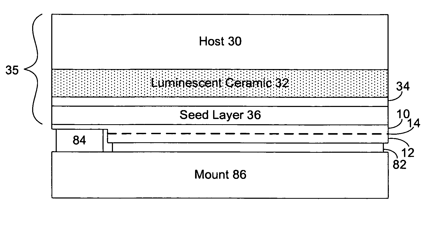
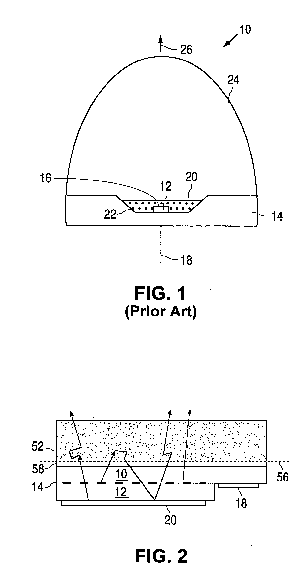
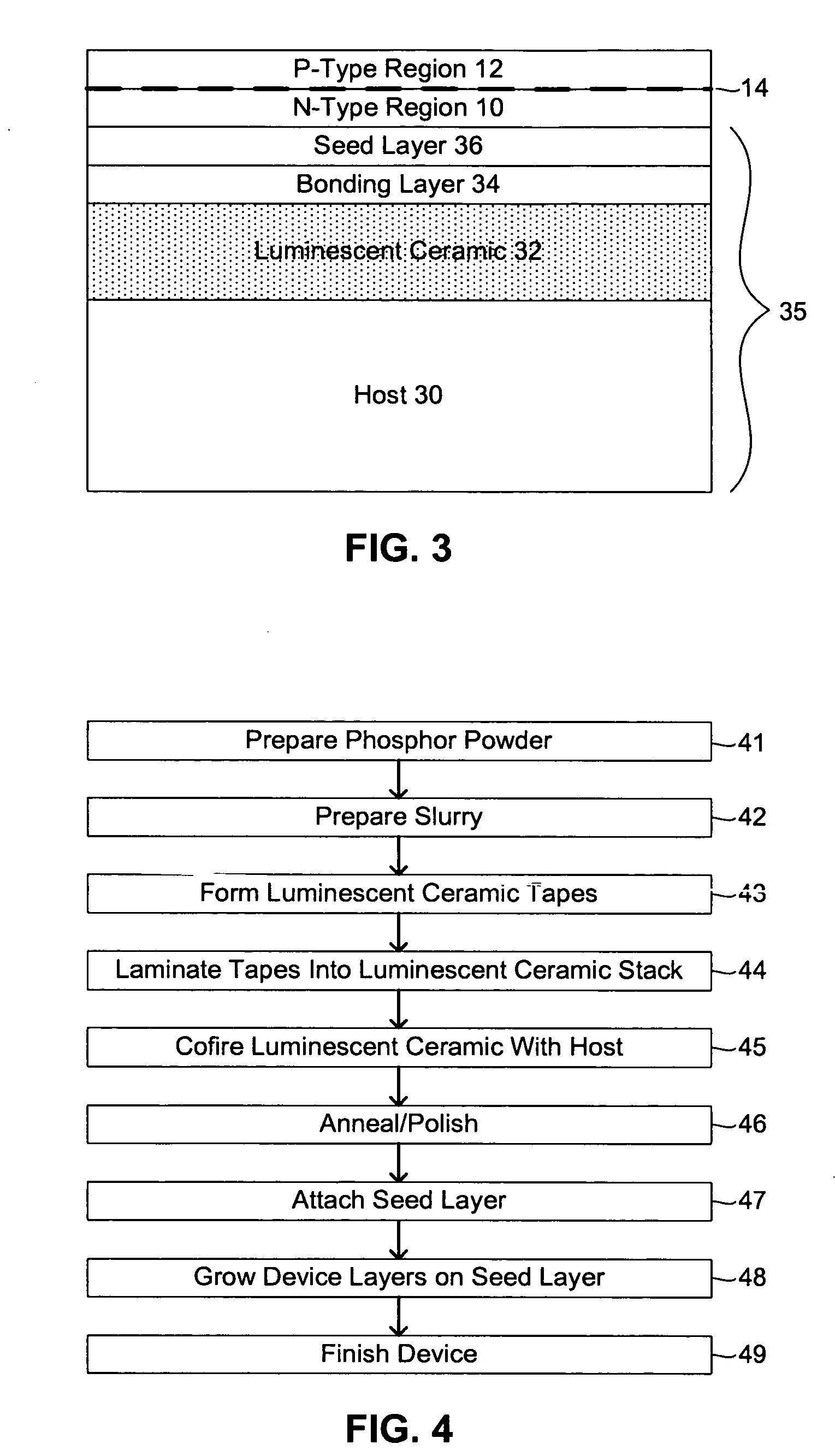
[0024] U.S. patent application Ser. No. 10 / 861,172, titled “Luminescent Ceramic for a Light Emitting Device,” filed Jun. 3, 2004 and incorporated herein by reference describes wavelength converting materials such as phosphors formed into ceramic slabs, referred to herein as “luminescent ceramics,”“ceramic layers” or “ceramic phosphors.” The ceramic slabs may be self-supporting layers formed separately from the semiconductor device, then attached to the finished semiconductor device or used as a growth substrate for the semiconductor device. The ceramic layers may be translucent or transparent, which may reduce the scattering loss associated with non-transparent wavelength converting layers such as conformal layers. Luminescent ceramic layers may be more robust than thin film or conformal phosphor layers. In addition, since luminescent ceramic layers are solid, it may be easier to make optical contact to additional optical elements such as lenses and secondary optics, which are also ...


PUM

PropertyMeasurementUnit
thicknessaaaaaaaaaa
thicknessaaaaaaaaaa
thicknessaaaaaaaaaa

Abstract

A semiconductor structure including a light emitting layer disposed between an n-type region and a p-type region is attached to a compound substrate including a host which provides mechanical support to the device and a ceramic layer including a luminescent material. In some embodiments the compound substrate includes a crystalline seed layer on which the semiconductor structure is grown. The ceramic layer is disposed between the seed layer and the host. In some embodiments, the compound substrate is attached to the semiconductor structure compound substrate is spaced apart from the semiconductor structure and does not provide mechanical support to the structure. In some embodiments, the ceramic layer has a thickness less than 500 μm.

Description

BACKGROUND [0001] 1. Field of Invention [0002] This invention relates to wavelength converting members suitable for use with semiconductor light emitting devices such as light emitting diodes. [0003] 1. Description of Related Art [0004] Semiconductor light-emitting devices including light emitting diodes (LEDs), resonant cavity light emitting diodes (RCLEDs), vertical cavity laser diodes (VCSELs), and edge emitting lasers are among the most efficient light sources currently available. Materials systems currently of interest in the manufacture of high-brightness light emitting devices capable of operation across the visible spectrum include Group III-V semiconductors, particularly binary, ternary, and quaternary alloys of gallium, aluminum, indium, and nitrogen, also referred to as III-nitride materials. Typically, III-nitride light emitting devices are fabricated by epitaxially growing a stack of semiconductor layers of different compositions and dopant concentrations on a sapphire,...

Claims


Application Information

Patent Timeline
Patent Type & Authority Applications(United States)
IPC IPC(8): H01L33/00H01L33/50
CPCC04B35/44C04B35/597H01L2924/0002C04B35/63416C04B35/645C04B2235/3208C04B2235/3224C04B2235/3225C04B2235/3229C04B2235/5445C04B2235/6025C04B2235/6581C04B2235/662C09K11/0883C09K11/7721C09K11/7731C09K11/7734C09K11/7774C09K11/7792H01L33/007H01L33/0079H01L33/502H01L2924/00H01L33/32H01L33/505H01L33/0093
Inventor KRAMES, MICHAEL R.SCHMIDT, PETER J.
Owner PHILIPS LUMILEDS LIGHTING CO LLC
Why Eureka
Try Eureka