Solid-state imaging device, line sensor and optical sensor and method of operating solid-state imaging device

Active Publication Date: 2007-06-14
TOHOKU UNIV
View PDF11 Cites 111 Cited by
  • Summary
  • Abstract
  • Description
  • Claims
  • Application Information

AI Technical Summary

Benefits of technology

[0071] According to the present invention, the solid-state imaging device enables the photodiode receiving light and generating the photoelectric charges to maintain a high sensitivity with a high S/N ratio during imaging at low illuminance and, further, the storage capacitor element to accumulate the photoelectric charges, overflowing from the photodiode, for enabling imaging at high illuminance, resulting in capability of enhancing a wide dynamic range.
[0072] With the line s

Problems solved by technology

However, according to the methods disclosed in the Patent Documents 1, 2, 3 and the Non-Patent Document 2, mentioned above, or the method of performing the double shooting for different exposure times, the shootings for low illuminance and high illuminance need to be performed at different times. Therefore, a difference exists in moving images resulting from the shootings performed in respective illuminance and an issue occurs with a difficulty caused in matching both of the images.
Further, with the methods disclosed in Patent-Document 4 and Non-Patent Document 3 mentioned above, even though a sche

Method used


Image

  • Solid-state imaging device, line sensor and optical sensor and method of operating solid-state imaging device
  • Solid-state imaging device, line sensor and optical sensor and method of operating solid-state imaging device
  • Solid-state imaging device, line sensor and optical sensor and method of operating solid-state imaging device

Examples


first embodiment

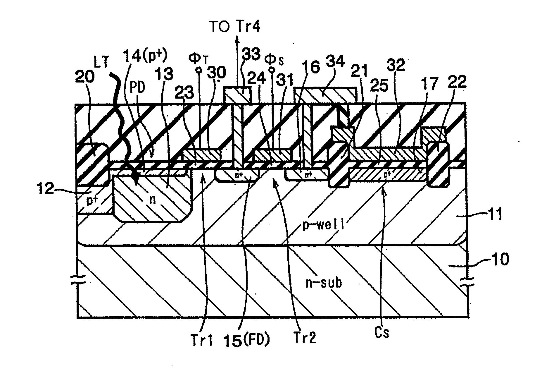
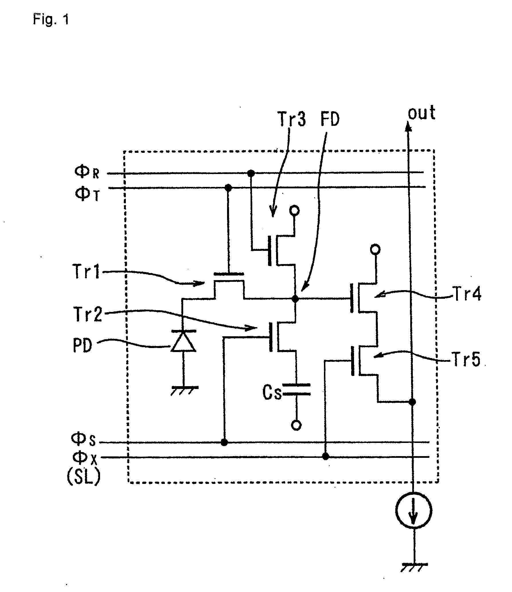
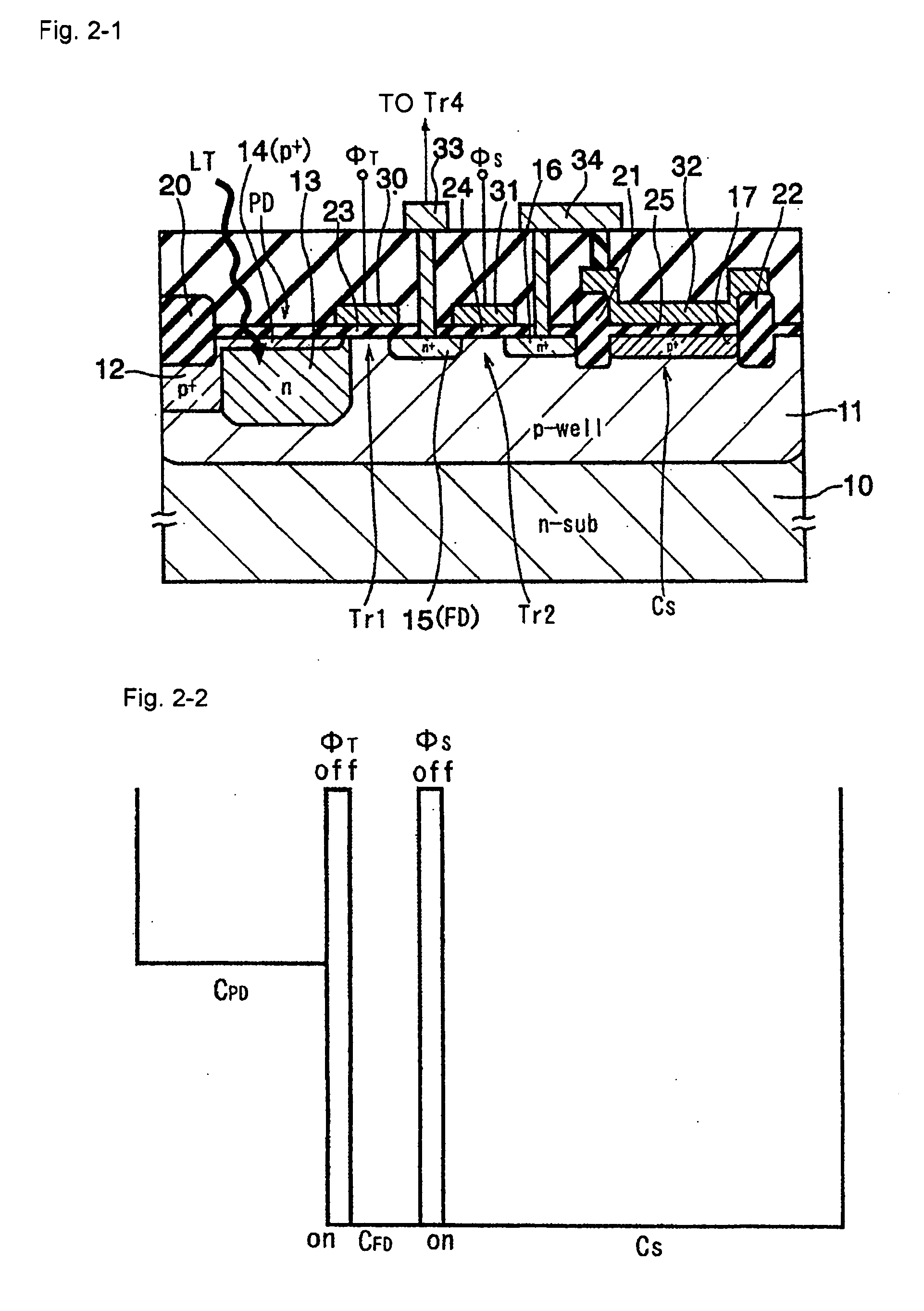
[0225] A solid-state imaging device of the present embodiment is structured in the form of a CMOS image sensor and FIG. 1 is an equivalent circuit diagram for one pixel.

[0226] Each pixel includes a photodiode PD for receiving light and generating photoelectric charges, a transfer transistor Tr1 for transferring the photoelectric charges of the photodiode PD, a floating region FD from which the photoelectric charges are transferred via the transfer transistor Tr1, a storage capacitor element Cs for accumulating the photoelectric charges overflowing from the photodiode during accumulating operation, a storage transistor Tr2 for coupling or splitting potentials of the floating region FD and the storage capacitor element Cs, a reset transistor Tr3 connected to the floating region FD for discharging the photoelectric charges of the floating region FD, an amplifier transistor Tr4 for amplifying the photoelectric charges of the floating region FD and converting to a voltage signal, and a ...

second embodiment

[0296] The present embodiment is a modified form of the circuit structure of pixels of the CMOS image sensor of the first embodiment.

[0297]FIG. 9-1 is an equivalent circuit diagram of an example of one pixel in the CMOS image sensor of the present embodiment. This embodiment is substantially Identical to the equivalent circuit diagram of FIG. 1 and differs from the same in connection between the amplifier transistor Tr4 and the selection transistor Tr5 in a form in which the selection transistor Tr5 is placed in an upper stage area of the amplifier transistor Tr4 and the output of the amplifier transistor Tr4 is connected to the output line “out”.

[0298] Such a connection makes it possible to raise a gain of an amplifier of the amplifier transistor Tr4.

[0299] Further, FIG. 9-2 is an equivalent circuit diagram of one pixel in the other example of the CMOS image sensor of the present embodiment. This embodiment is substantially identical to the equivalent circuit diagram of FIG. 1 b...

third embodiment

[0303] A solid-state imaging device of the present embodiment takes the form of a CCD image sensor.

[0304]FIG. 10-1 is an equivalent circuit diagram of an example of one pixel in the CCD image sensor of the present embodiment.

[0305] Specifically, first and second charge-couple transfer paths CCD1 and CCD2 are placed in vertically extending directions and driven in two phases with φV1 and φV2. A photodiode PD is directly connected to the first charge-couple transfer path CCD1 and connected to the second charge-couple transfer path CCD2 via a transfer transistor Tr1.

[0306] Herein, the second charge-couple transfer path CCD2 functions as a storage capacitor element C that accumulates photoelectric charges, overflowing from the photodiode, when the photodiode PD is saturated.

[0307] In the CCD image sensor of the structure previously mentioned, the first charge-couple transfer path CCD1 transfers pre-saturated charges in low illuminance for readout upon driving CCD. In the meanwhile, ...


PUM


Abstract

A solid-state imaging device, a line sensor and an optical sensor for enhancing a wide dynamic range while keeping high sensitivity with a high S/N ratio, and a method of operating a solid-state imaging device for enhancing a wide dynamic range while keeping high sensitivity with a high S/N ratio are provided. The solid-state imaging device comprises an integrated array of a plurality of pixels, each of which comprises a photodiode PD for receiving light and generating photoelectric charges, a transfer transistor Tr1 for transferring the photoelectric charges, and a storage capacitor element C connected to the photodiode PD at least through the transfer transistor Tr1 for accumulating, at least through the transfer transistor Tr1, the photoelectric charge overflowing from the photodiode PD during accumulating operation.

Description

TECHNICAL FIELD [0001] The present invention relates to solid-state imaging devices, line sensors and optical sensors and methods of operating the solid-state imaging devices and, more particularly, to a solid-state imaging device, a line sensor and an optical sensor of a CMOS type or a CCD type and a method of operating the solid-state imaging device. BACKGROUND ART [0002] Image-input image sensors such as CMOS (Complementary Metal-Oxide-Semiconductor) image sensors or CCD (Charge Coupled Device) image sensors have achieved improvements in characteristics with an expanding, demand for applications in, for instance, digital cameras and cellular phones each with a camera. [0003] The image sensors, described above, need to be further improved in characteristics, one of which relates to widening a dynamic range. [0004] The image sensor has heretofore been used in the related art and has a dynamic range in the order of, for instance, approximately 3 to 4 digits (60 to 80 dB) under an ac...

Claims


Application Information

Patent Timeline
IPC IPC(8): H01L31/113H01L27/146H04N1/028H04N5/335H04N5/347H04N5/355H04N5/357H04N5/369H04N5/374H04N5/3745
CPCH01L27/14603H01L27/14609H01L27/1463H04N5/3559H04N5/374H04N5/37452H04N25/59H04N25/76H04N25/771H01L27/146
Inventor SUGAWA, SHIGETOSHI
Owner TOHOKU UNIV
Why Eureka
Try Eureka