Laser fuse with efficient heat dissipation

Active Publication Date: 2007-06-14
TAIWAN SEMICON MFG CO LTD
View PDF12 Cites 15 Cited by
  • Summary
  • Abstract
  • Description
  • Claims
  • Application Information

AI Technical Summary

Benefits of technology

[0015] The advantageous features of the preferred embodiments of the present invention include reducing peeling an

Problems solved by technology

Even if only one memory cell has defects, the entire chip may be rendered defective.
Highly integrated semiconductor memory devices have a fairly high manufacturing cost, which causes a big loss if any defective cells are discovered.
Mechanical stress and heat generated by laser processes damage the underlying structures an

Method used


Image

  • Laser fuse with efficient heat dissipation
  • Laser fuse with efficient heat dissipation
  • Laser fuse with efficient heat dissipation

Examples


Example

[0020] The making and using of the presently preferred embodiments are discussed in detail below. It should be appreciated, however, that the present invention provides many applicable inventive concepts that can be embodied in a wide variety of specific contexts. The specific embodiments discussed are merely illustrative of specific ways to make and use the invention, and do not limit the scope of the invention.

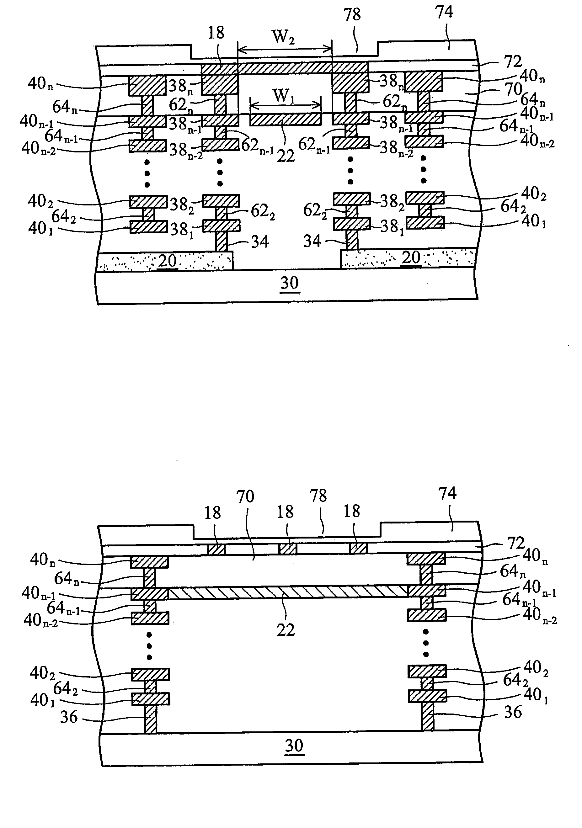
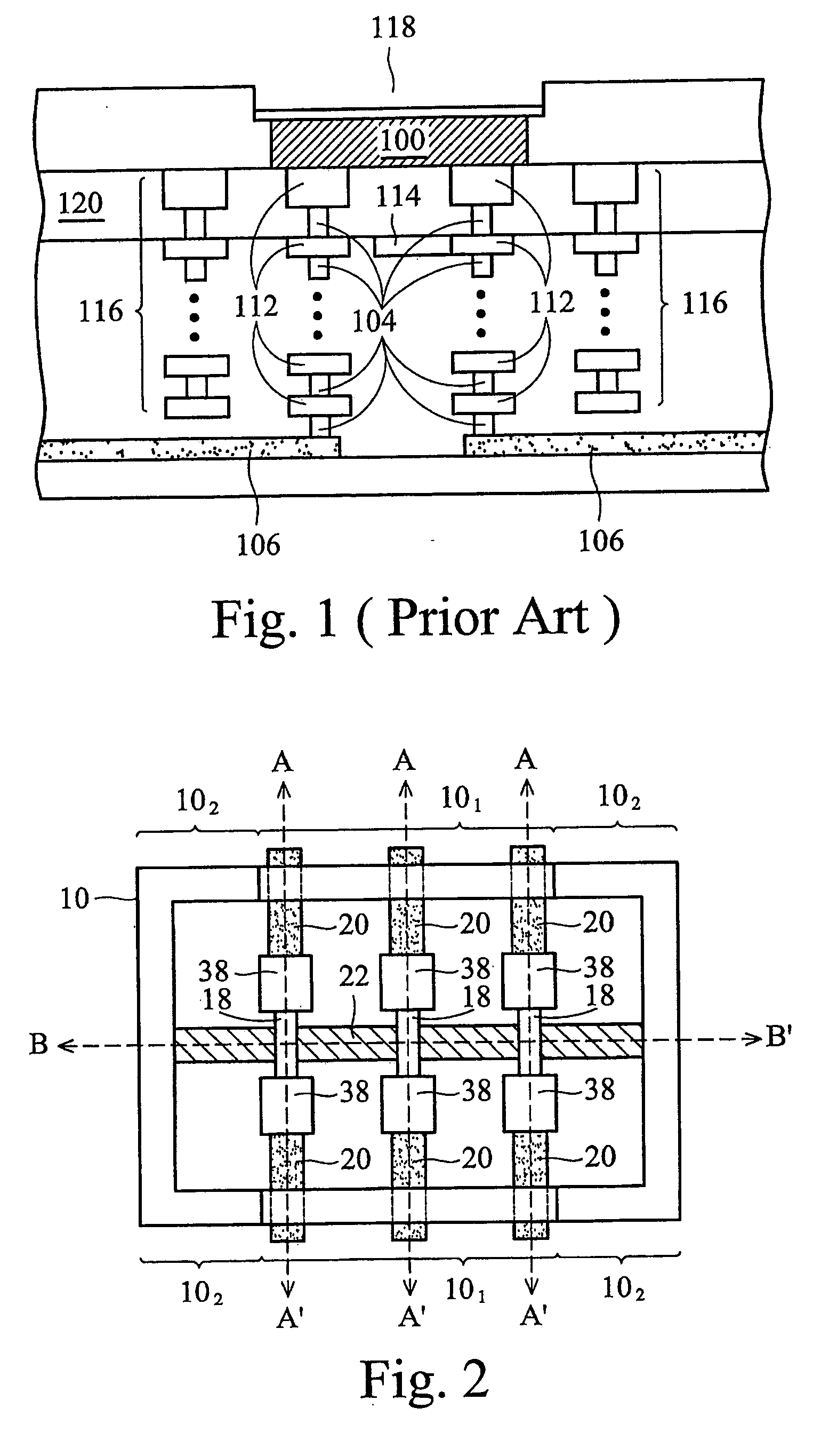
[0021]FIG. 2 illustrates a top view of the preferred embodiment of the present invention. For illustration purposes, features in different layers are shown in one plane. One skilled in the art will realize that these features may range from a top metallization layer to a substrate. A protection ring 10, which comprises portions 101 and 102, encloses one or more laser fuses 18, which are located over the top metallization layer (referred to as Mn) (not shown). Fuses 18 are connected to electrical circuits through conductive lines 20, which are preferably formed of polysilico...


PUM


Abstract

A semiconductor structure having an efficient thermal path and a method for forming the same are provided. The semiconductor structure includes a protection ring over a semiconductor substrate and substantially encloses a laser fuse structure. The laser fuse structure includes a laser fuse and a connection structure connecting the fuse to integrated circuits. The protection ring is thermally coupled to the semiconductor substrate by contacts. The semiconductor structure further includes a metal plate conducting heat generated by a laser beam to the protection ring.

Description

TECHNICAL FIELD [0001] This invention relates generally to laser fuses in integrated circuits, and more particularly to structures and methods for protecting integrated circuits from damage caused by laser fuse burning. BACKGROUND [0002] A typical integrated circuit may include millions of devices or sub circuits. Some of the integrated circuits contain a lot of identical sub circuits. For example, a memory chip contains a lot of identical memory cells. Even if only one memory cell has defects, the entire chip may be rendered defective. [0003] To increase yield, redundant memory cells are manufactured on the same chip. If some of the primary memory cells have defects, redundant memory cells can be used to replace the defective primary memory cells. This redundant configuration permits the semiconductor memory device to continue to operate in a normal state. The primary memory cells and redundant memory cells are all connected via fuses controlled by control circuits on the chip. As ...

Claims


Application Information

Patent Timeline
IPC IPC(8): H01L29/00
CPCH01L23/5258H01L2924/0002H01L2924/00
Inventor TSAI, HAO-YIYANG, CHAO-HSIANGHOU, SHANG-YUNTSAI, CHIA-LUNJENG, SHIN-PUU
Owner TAIWAN SEMICON MFG CO LTD
Why Eureka
Try Eureka