
Organic electro-luminescence display device and method for fabricating the same

Active Publication Date: 2007-06-14
LG DISPLAY CO LTD
View PDF4 Cites 56 Cited by
  • Summary
  • Abstract
  • Description
  • Claims
  • Application Information

AI Technical Summary

Benefits of technology

[0012] An object of embodiments of the invention is to provide an organic electro-luminescence display device and a method for fabricating the same that increase production yield, reduce defect rate, and improve product management efficiency.
[0013] Another object of the invention is to provide an organic electro-luminescence display device and a method for fabricating the same that have improved light efficiency.
[0014] Another object of the invention is to provide an organic electro-luminescence display device and a method for fabricating the same that have a simplified fabrication process with reduced number of masks.

Problems solved by technology

Thus, the yield of an entire process is considerably limited by a manufacturing process of the OLED.
For example, even when the array device is properly formed, the organic electro-luminance display device is considered as a defective device when a defect is generated by foreign substances or other factors while an organic light-emitting layer using a thin film of about 1000 Å is formed.
Accordingly, a loss in the related costs and material costs consumed for manufacturing a good array device is generated, to thereby reduce product yield.
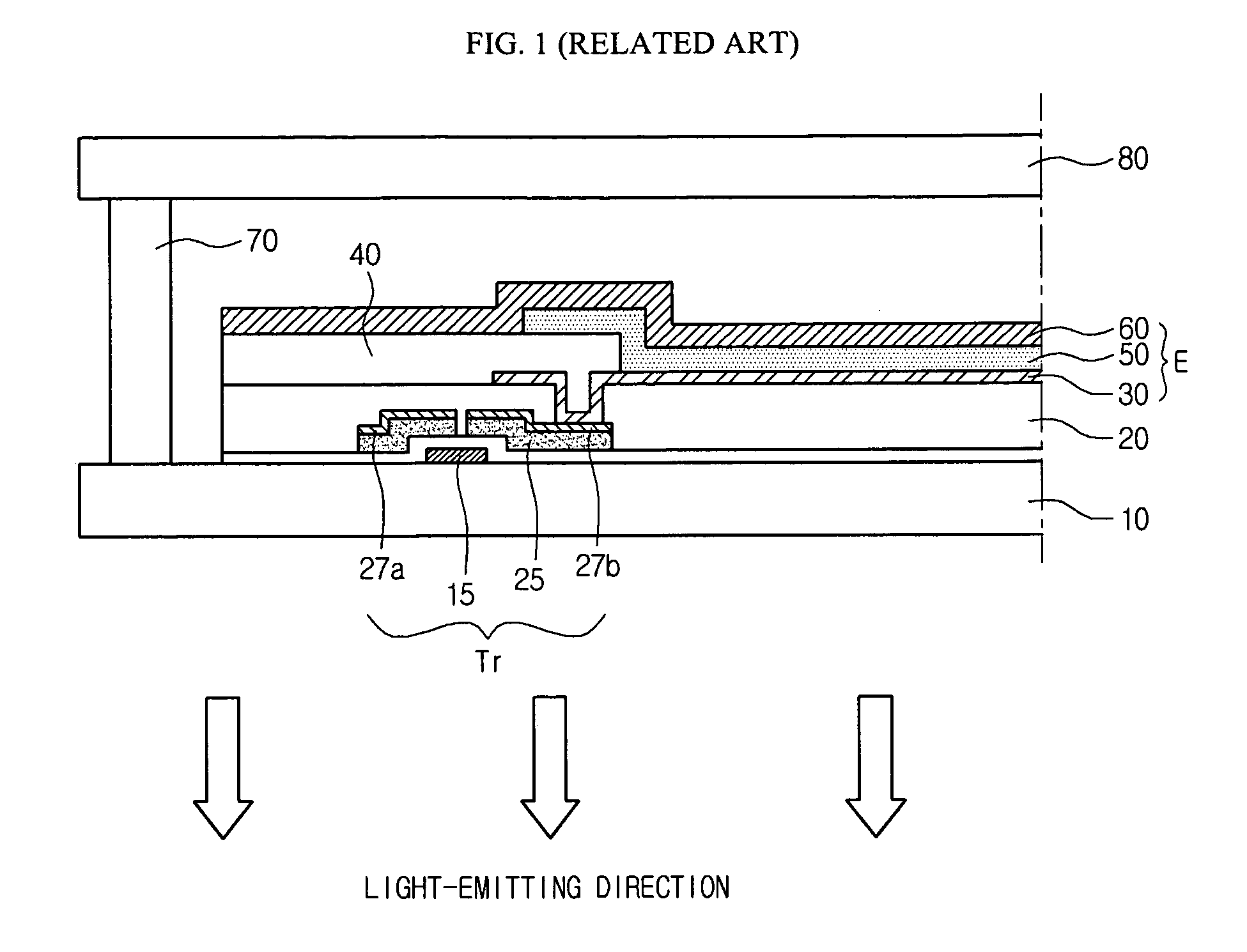
In addition, although the related art organic electro-luminance display device has stability by an encapsulation process and a high degree of freedom in a process, there exists a limitation in an aperture.
Therefore, it is difficult to fabricate the related art organic electro-luminance display device as a high resolution display device.

Method used


Image

  • Organic electro-luminescence display device and method for fabricating the same
  • Organic electro-luminescence display device and method for fabricating the same
  • Organic electro-luminescence display device and method for fabricating the same

Examples


Embodiment Construction

[0028] Reference will now be made in detail to the preferred embodiments of the invention, examples of which are illustrated in the accompanying drawings.

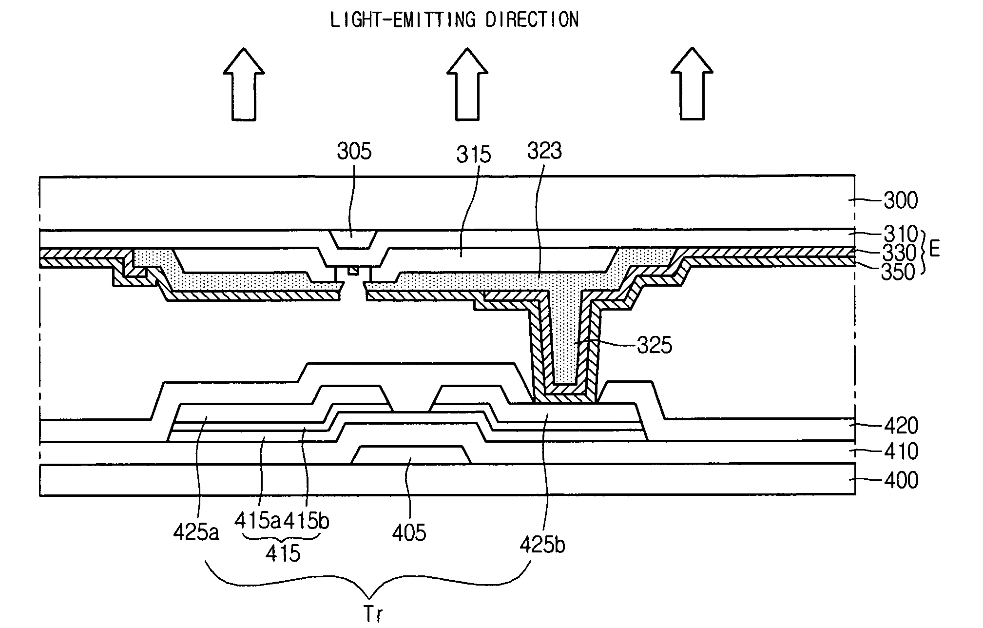
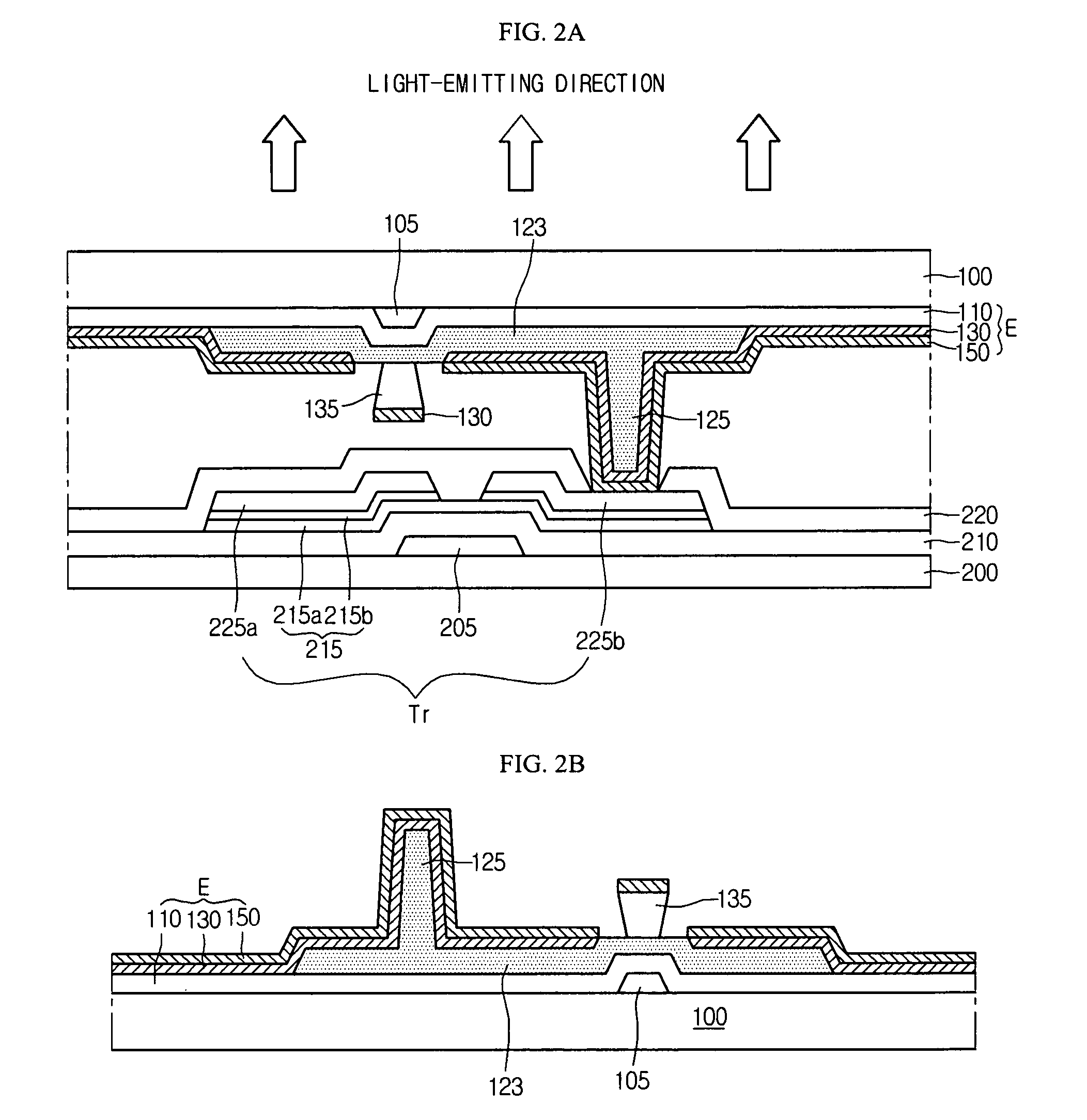
[0029]FIGS. 2A to 2C are cross-sectional schematic diagrams an organic electro-luminescence display device according to an embodiment of the invention. In FIG. 2A, an organic electro-luminescence display device includes a first substrate 100 and a second substrate 200. The first and second substrates 100 and 200 face each other with a predetermined interval interposed therebetween. An OLED E is formed in a sub-pixel on the first substrate 100, and an array device including a thin film transistor (TFT) Tr is formed corresponding to the OLED E on the second substrate 200. A spacer 125 for maintaining a gap is interposed between the first substrate 100 and the second substrate 200. The OLED is electrically connected to the TFT Tr by the spacer 125. The OLED E emits light using a voltage applied in response to a switching control of t...


PUM


Abstract

An organic electro-luminance display device includes a first substrate including a plurality of sub-pixels, a first electrode on the first substrate, a buffer layer on the first electrode of a region that partitions each of the sub-pixels, a spacer on the buffer layer, the buffer layer and the spacer being integrally formed, an organic light-emitting layer on the first electrode that corresponds to each of the sub-pixels and the spacer, and a second electrode on the organic light-emitting layer.

Description

[0001] The invention claims the benefit of Korean Patent Application No. 123079 / 2005 filed in Korea on Dec. 14, 2005, which is hereby incorporated by reference in its entirety. BACKGROUND OF THE INVENTION [0002] 1. Field Of The Invention [0003] The invention relates to a flat panel display device, and more particularly, to an organic electro-luminescence display device and a method for fabricating the same. Although embodiments of the invention is suitable for a wide scope of applications, it is particularly suitable for increasing production yield in fabricating an organic electro-luminescence device and for improving light efficiency in an organic electro-luminescence display device. [0004] 2. Discussion Of The Related Art [0005] An electro-luminescence display device generates light based on the principle of electroluminescence. An exciton which consists of an excited electron-hole pair, is generated inside an emissive layer, and when the exciton's electron and hole combine, a ph...

Claims


Application Information

Patent Timeline
IPC IPC(8): H01J9/24H01J1/62
CPCH01L27/3246H01L27/3253H10K59/1275H10K59/122H05B33/22H05B33/10
Inventor PARK, JONG WOO
Owner LG DISPLAY CO LTD
Learn More