Semiconductor device and manufacturing method therefor

a technology of semiconductor devices and manufacturing methods, applied in the direction of semiconductor devices, basic electric elements, electrical appliances, etc., can solve the problems of difficult to form a so-called dual work function metal gate, difficult to control the nisix composition with precision and ease, etc., to achieve a uniform metal composition ratio and control the metal composition with ease

Inactive Publication Date: 2007-06-21
RENESAS TECH CORP
View PDF4 Cites 11 Cited by
  • Summary
  • Abstract
  • Description
  • Claims
  • Application Information

AI Technical Summary

Benefits of technology

[0013]Therefore, it is an object of the present invention to provide a semiconductor device and a manufacturing method therefor, the semiconductor device including fu

Problems solved by technology

Since a gate electrode typically has a height substantially larger than the thickness of NiSix required for the source/drain region, NiSix formed on the source/drain region simultaneously with the full silicidation of the gate electrode has an excessively large thickness, which causes a device characteristic problem.
Further, in some cases, cubical expansion becomes significant, resulting in protrusion of NiSix to the upper portion of the gate electrode or penetration of NiSix through the insulating film to reach

Method used


Image

  • Semiconductor device and manufacturing method therefor
  • Semiconductor device and manufacturing method therefor
  • Semiconductor device and manufacturing method therefor

Examples


first embodiment

A. Configuration

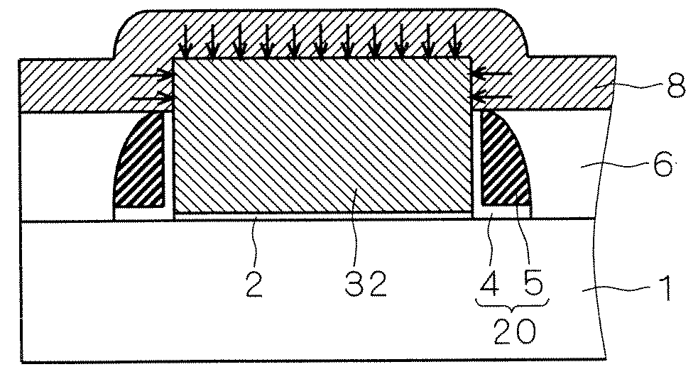
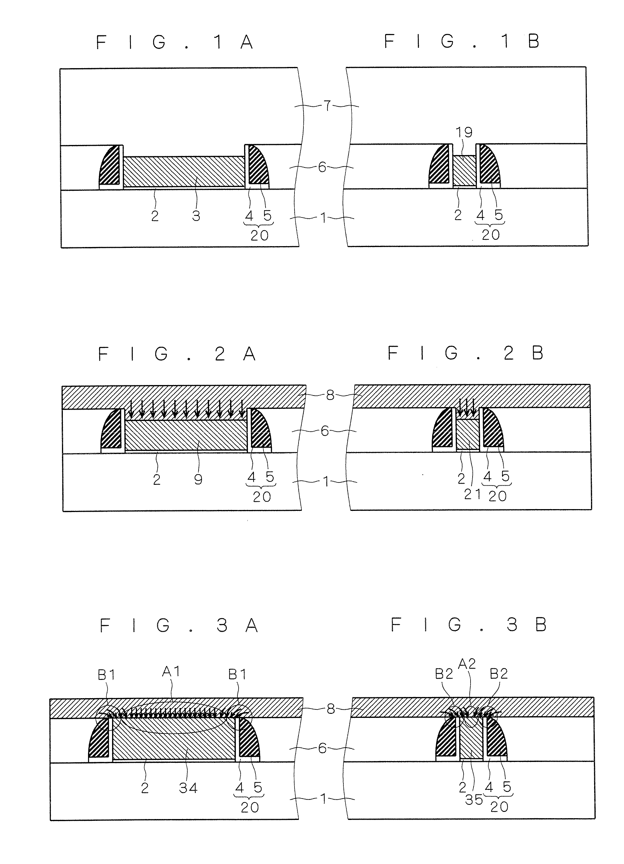
[0042]FIGS. 1A and 1B are sectional views showing a configuration of a semiconductor device according to a first embodiment. As shown in FIG. 1A, a MISFET with a large gate length and a MISFET (FIG. 1B) with a fine gate length are formed in the semiconductor device according to the first embodiment.

[0043]An interlayer insulating film 6 is formed on a semiconductor substrate 1. Full silicide gate electrodes (also referred to as metal gate electrodes) 3, 19 which are fully silicided are formed inside the interlayer insulating film 6 on the semiconductor substrate 1 via a gate insulating film 2.

[0044]The full silicide gate electrode 3 is formed on the gate insulating film 2 in the MISFET with a large gate length. Further, the full silicide gate electrode 19 is formed on the gate insulating film 2 in the MISFET with a fine gate length.

[0045]Here, each of the full silicide gate electrodes 3, 19 is a gate electrode fully silicided from its upper portion to its face (bottom...

second embodiment

[0066]A semiconductor device according to a second embodiment is one obtained by applying the first embodiment to a CMOS structure.

A. Configuration

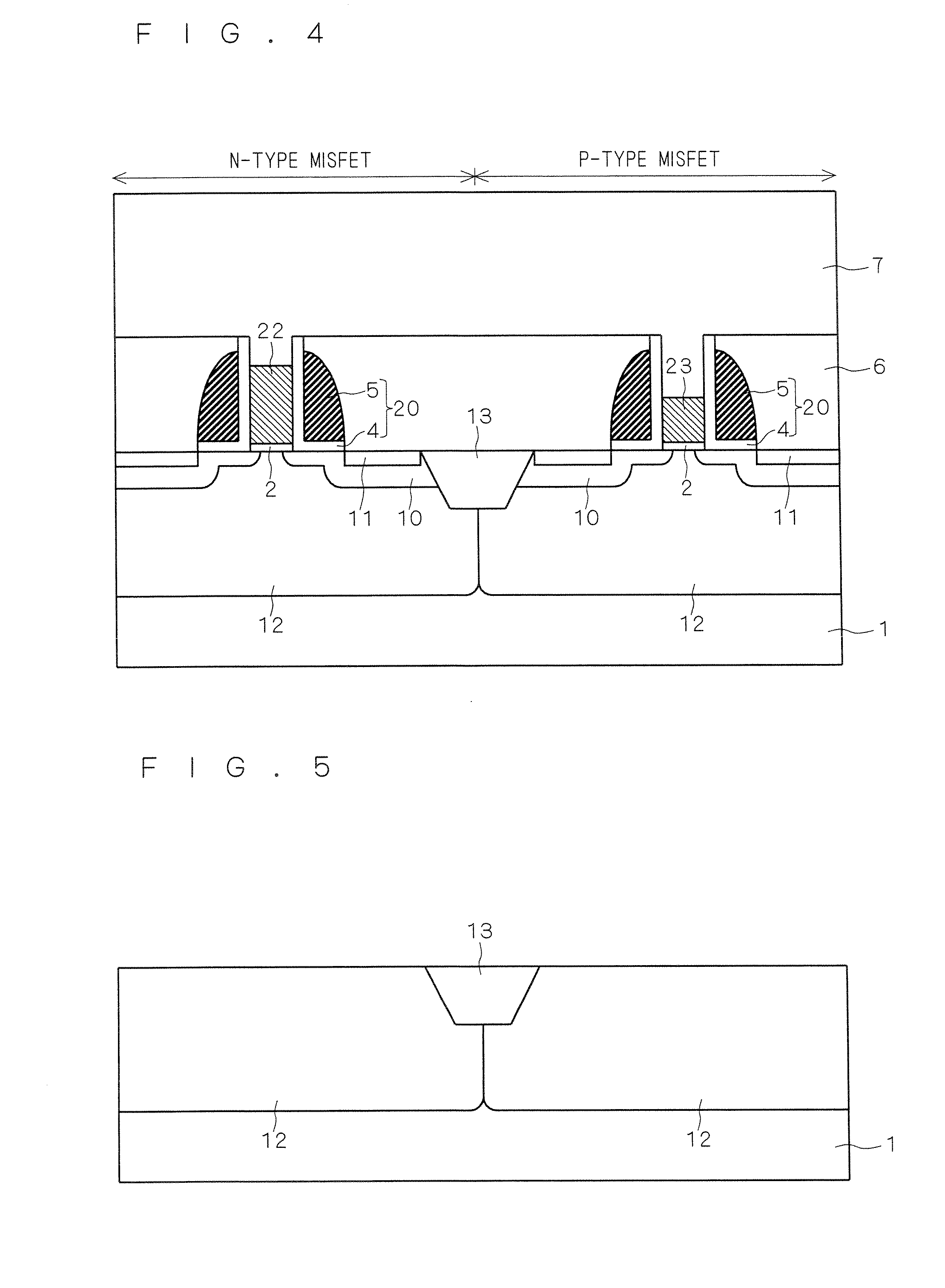
[0067]FIG. 4 is a sectional view showing a configuration of the semiconductor device according to the second embodiment. The semiconductor device according to the second embodiment includes a COMS configuration in which an N-type MISFET (nFET) and a P-type MISFET (pFET) are formed.

[0068]As shown in FIG. 4, the nFET and the pFET are separated from each other by an STI (shallow trench isolation) 13. Well regions 12 are formed on the upper layer portion of the semiconductor substrate 1. A source / drain region 10 is formed on the upper layer portion of the well regions 12.

[0069]The interlayer insulating film 6 is formed on the semiconductor substrate 1. In the nFET formation region, a full-silicide gate electrode 22 is formed inside the interlayer insulating film 6 on the semiconductor substrate 1 via the gate insulating film 2. Further, in th...

third embodiment

A. Configuration

[0110]FIGS. 13A and 13B are sectional views showing a configuration of a semiconductor device according to a third embodiment. As shown in FIG. 13A, a MISFET with a large gate length and a MISFET (FIG. 13B) with a fine gate length are formed in the semiconductor device according to the third embodiment.

[0111]The interlayer insulating film 6 is formed on the semiconductor substrate 1. Full silicide gate electrodes (also referred to as metal gate electrodes) 30, 31 which are fully silicided are formed inside the interlayer insulating film 6 on the semiconductor substrate 1 via the gate insulating film 2.

[0112]The full silicide gate electrode 30 is formed on the gate insulating film 2 in the MISFET with a large gate length. Further, the full silicide gate electrode 31 is formed on the gate insulating film 2 in the MISFET with a fine gate length.

[0113]Here, each of the full silicide gate electrodes 30, 31 is a gate electrode fully silicided from its upper portion to its ...


PUM


Abstract

The top ends of polysilicon gate electrodes with different gate lengths are formed so as to be equally high and lower than the top end of the side wall. A metal film is formed so as to cover the polysilicon gate electrodes, followed by silicidation by thermal treatment. Since the top ends of the polysilicon gate electrodes are formed lower than the top end of the side wall, a silicon side reaction is not accelerated even in the case of a fine gate length, and proceeds in a one-dimensional manner. As a result, full-silicide gate electrodes having a uniform metal composition ratio can be stably formed even using the polysilicon gates with different gate lengths.

Description

BACKGROUND OF THE INVENTION[0001]1. Field of the Invention[0002]The present invention relates to a semiconductor device, and a manufacturing method therefor. In particular, the present invention relates to a semiconductor device including a MISFET which includes a fully silicided gate electrode, and a manufacturing method therefor.[0003]2. Description of the Background Art[0004]In Japanese Patent Application Laid-Open No. 11-284179 (1999), there is provided a so-called full silicide (FUSI) technique as a technique capable of relatively easily preparing a metal gate. In this technique, polysilicon is formed as a gate electrode up to a source / drain region in the same manner as in a normal MISFET formation flow, and a metal such as Ni is then deposited on the polysilicon. Subsequently, the metal is reacted with Si by annealing to fully silicide the polysilicon for formation of a full-silicide gate electrode.[0005]At this time, NiSix is also formed on the source / drain region simultaneou...

Claims


Application Information

Patent Timeline
IPC IPC(8): H01L29/76
CPCH01L21/28114H01L21/823443H01L21/823456H01L21/823468H01L21/823835H01L21/82385H01L21/823864H01L29/42376H01L29/6653H01L29/66545H01L29/6656
Inventor EIKYU, KATSUMIYAMASHITA, TOMOHIROHORITA, KATSUYUKIHAYASHI, TAKASHI
Owner RENESAS TECH CORP
Why Eureka
Try Eureka