Methods to prepare silicon-containing films

a technology of silicon-containing films and compositions, applied in chemical/physical/physicochemical processes, organic chemistry, coatings, etc., can solve the problems of undesirable elements in films, detrimental to the photolithographic patterning process of semiconductor devices, and inability to accurately form features, etc., to achieve high purity

Active Publication Date: 2014-04-22
VERSUM MATERIALS US LLC
View PDF28 Cites 0 Cited by
  • Summary
  • Abstract
  • Description
  • Claims
  • Application Information

AI Technical Summary

Benefits of technology

[0010]In alternative embodiments, the method and precursor described herein can provide a material having a relatively low nitrogen content which provides a nitrogen-doped oxide material with a controlled composition. In alternative embodiments, the method and precursor described herein can provide a material having a relatively low carbon content which provides a carbon-doped oxide material with a controlled composition. In these embodiments, the material may comprise from about 0 to about 30 atomic weight percent nitrogen and / or carbon as measured by XPS. In certain embodiments, the precursors used are capable of making SiO2 materials of very high purity, with non-detectable amounts of other elements including carbon, nitrogen, chlorine and halogens, and other species quantifiable by XPS.

Problems solved by technology

Depending upon the application, however, certain elements in the film may be undesirable even at lower concentration levels.
This may be detrimental to photolithographic patterning process of the semiconductor devices.
Photoresist poisoned material that subjected to typical patterning steps could result in imprecisely formed features in the photoresist or excessive residual photoresist after patterning, both of which can detrimentally affect PR processes, such as etch processes.
For example, nitrogen may neutralize acid near a photoresist and ARC interface and result in residue formation, known as footing, which can further result in curved or round aspects at the interface of the bottom and sidewalls of features rather than desired right angle.
However, the film quality of the PECVD TEOS film may be poorer because the films do not have a stoichiometric composition, are hydrogen-rich, have a low film density, and / or exhibit a fast etch rate.

Method used


Image

  • Methods to prepare silicon-containing films
  • Methods to prepare silicon-containing films
  • Methods to prepare silicon-containing films

Examples


example 1

Deposition of Silicon Oxide Films by Chemical Vapor Deposition Using Di-Tert-Butoxysilane (DTBOS)

[0082]Exemplary silicon oxide films were deposited using the precursors DTBOS and oxygen as the oxygen source. The deposition conditions for each film are provided in Table 1. The characteristics of each film are provided in Table 2.

[0083]

TABLE 1Depo-PrecursorDepo-sitionFlowPrecursorOxygensitionExemplaryTemp.PressureSettingFlowFlowTimeFilm(° C.)(mtorr)(%)(sccm)(sccm)(min.)15502503014.11205026502503014.11405036005003012.67409946505003013.46409956502503014.26409966502503010.464030sccm = standard cubic centimeters per minute

[0084]

TABLE 2AverageRefractiveExem-FilmFilmIndexDepositionplaryThicknessThicknessRefractiveUniformityRateFilm(Å)UniformityIndex(%)(Å / min.)11151.701.33186.00572.3025551.461.47330.202211.1035541.091.47340.21565.5945481.461.47190.26505.5655821.401.44480.25795.8761474.441.42493.01164.89

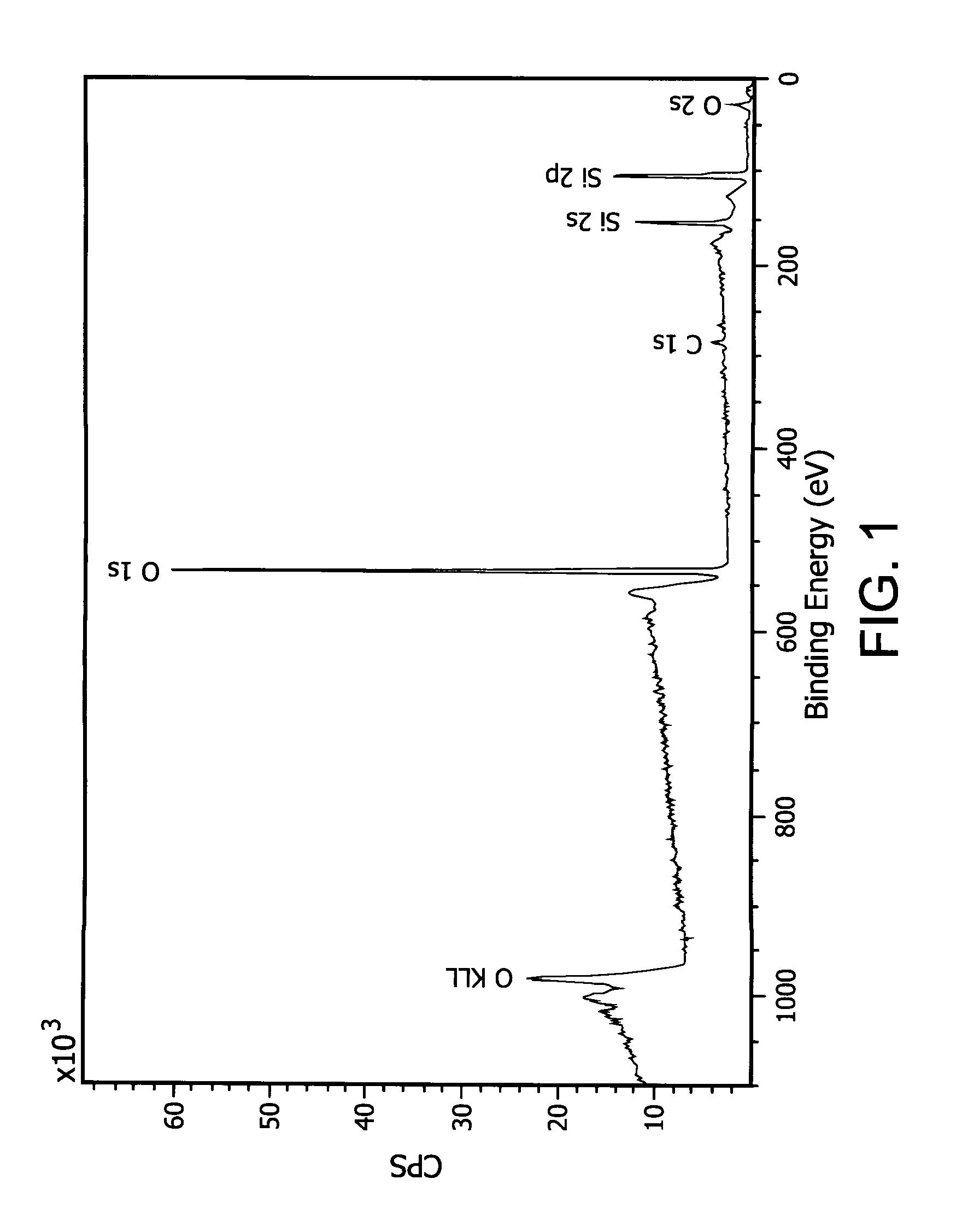
[0085]A typical XPS of one or the exemplary films from Example 1 that is highly uniform, h...

example 2

The Thickness Uniformity of the Film

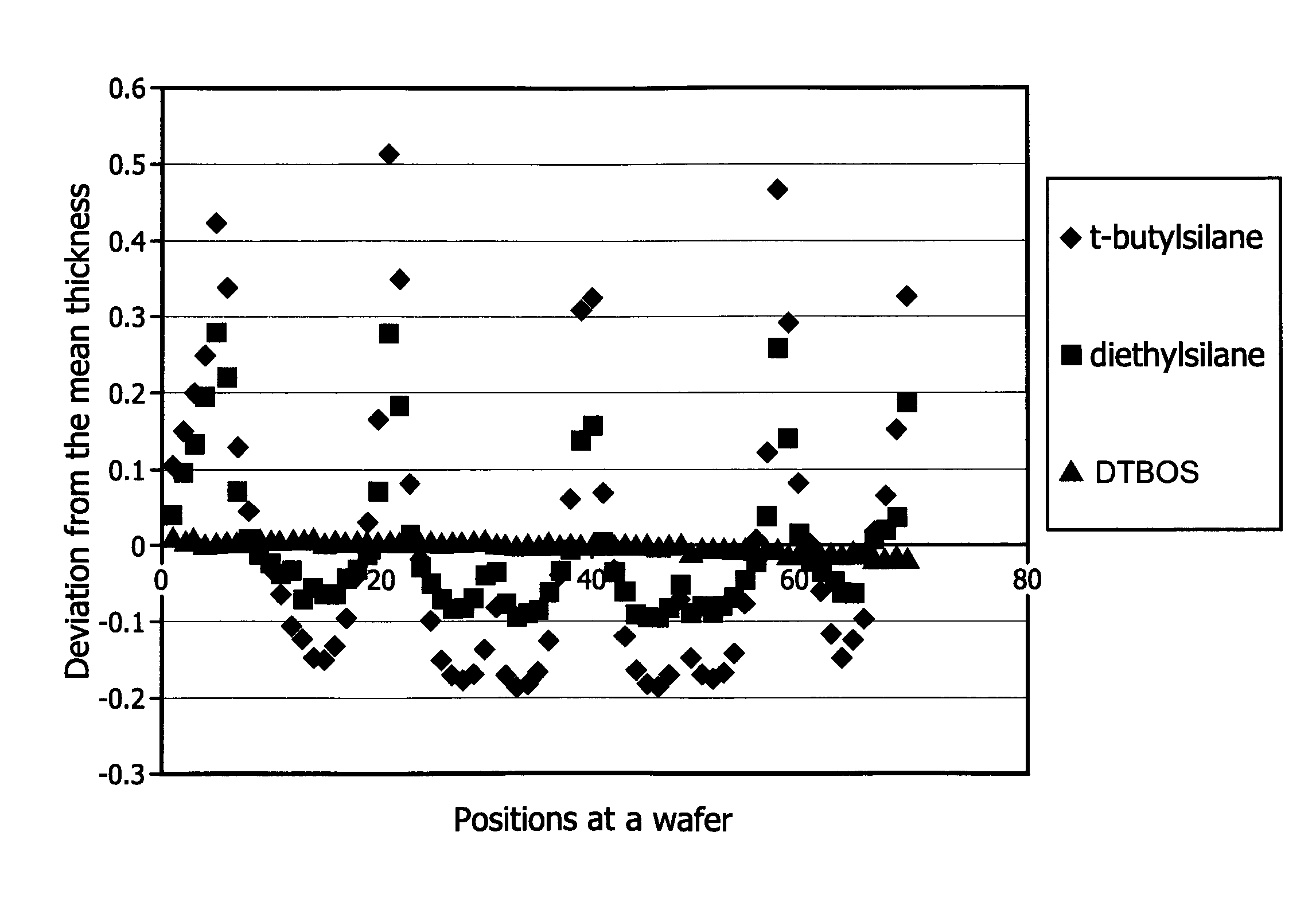
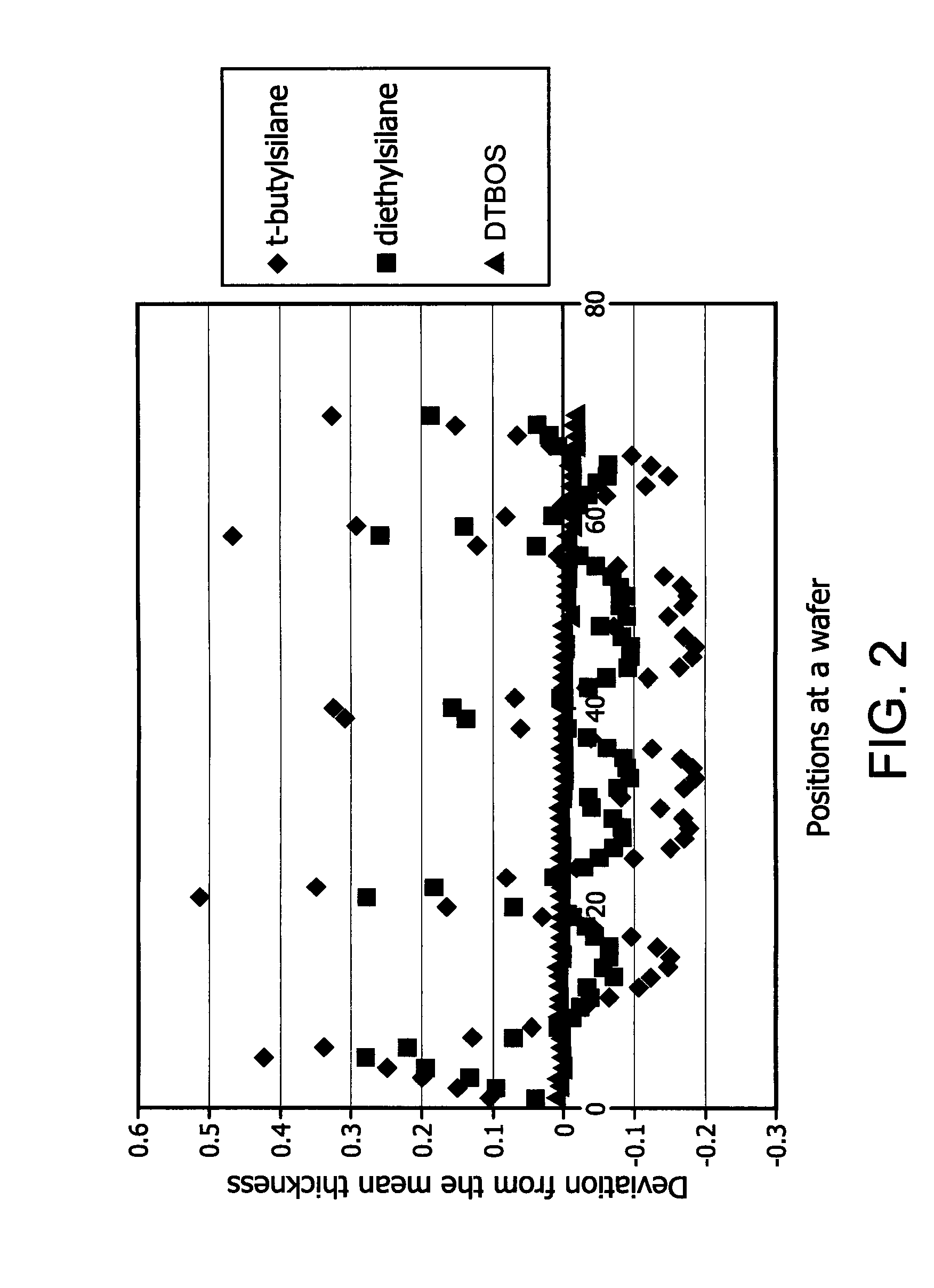
[0087]The nitrogen free silicon dioxide films formed using the methods and compositions described herein are measured for their thickness using an ellipsometer. In contrast to the poor uniformity of the nitrogen silicon dioxide films deposited using currently available methods, the films deposited using methods described in this invention show drastic improvement in the film uniformity within a substrate (or a wafer). A comparison in the film thickness uniformity between the films used the said invention and the ones used the existing methods is provided in FIG. 2 where the x-axis represents the position of measurement at a wafer substrate and y-axis represents the deviation of the thickness at each point from the average thickness of the film. It can be seen from FIG. 2 that the film deposited using the method described herein is much more uniform across the wafer substrates compared to other films.

A commonly used formula for thickness uniformity...

example 3

K And Dielectric Constant

[0090]The dielectric constant of the silicon oxide film formed using the method described herein is derived from the C-V plot shown in FIG. 3. For a known thickness of the film and contact area of the mercury probe used, the dielectric constant of the film is found to be 4.47.


PUM

PropertyMeasurementUnit
temperaturesaaaaaaaaaa

Abstract

Described herein are methods of forming dielectric films comprising silicon, oxide, and optionally nitrogen, carbon, hydrogen, and boron. Also disclosed herein are the methods to form dielectric films or coatings on an object to be processed, such as, for example, a semiconductor wafer.

Description

CROSS REFERENCE TO RELATED APPLICATION[0001]The present patent application claims the benefit of prior U.S. Provisional Patent Application Ser. No. 61 / 301,375 filed Feb. 4, 2010.BACKGROUND OF THE INVENTION[0002]Disclosed herein are methods and compositions to prepare silicon-containing materials or films, such as but not limited to, stoichiometric or non-stoichiometric silicon oxide, silicon oxynitride, or silicon oxycarbonitride films, for use in various electronic applications.[0003]Thin films of silicon oxide are commonly used as dielectrics in semiconductor manufacturing because of their dielectric properties. In the manufacturing of silicon-based semiconductor devices, silicon oxide films can be used as gate insulations, diffusion masks, sidewall spacers, hard mask, anti-reflection coating, passivation and encapsulation, and a variety of other uses. Silicon oxide films are also becoming increasingly important for passivation of other compound semiconductor devices.[0004]Other e...

Claims


Application Information

Patent Timeline
Patent Type & Authority Patents(United States)
IPC IPC(8): H01L23/58H01L21/36H01L21/20
CPCC23C16/44C09D183/04H01L21/316B01J19/00C07F7/02C23C16/30H01L29/00H01L21/02274H01L21/02164H01L21/02216H01L21/0228C23C16/50H01L21/0262C23C16/45553C23C16/401C23C16/455H01L21/20
Inventor YANG, LIUXIAO, MANCHAOHAN, BINGCUTHILL, KIRK S.O'NEILL, MARK L.
Owner VERSUM MATERIALS US LLC
Why Eureka
Try Eureka