

Device with beam structure, and semiconductor device
a beam structure and semiconductor technology, applied in the direction of semiconductor devices, piezoelectric/electrostrictive/magnetostrictive devices, semiconductor/solid-state device details, etc., can solve the problem of difficult to equalize the values of residual stresses in the respective layer, the capacitance value of the variable capacitor cannot be varied at a desired voltage value, and the desired capacitance value cannot be obtained
- Summary
- Abstract
- Description
- Claims
- Application Information
AI Technical Summary
Problems solved by technology
Method used
Image

Examples
first embodiment
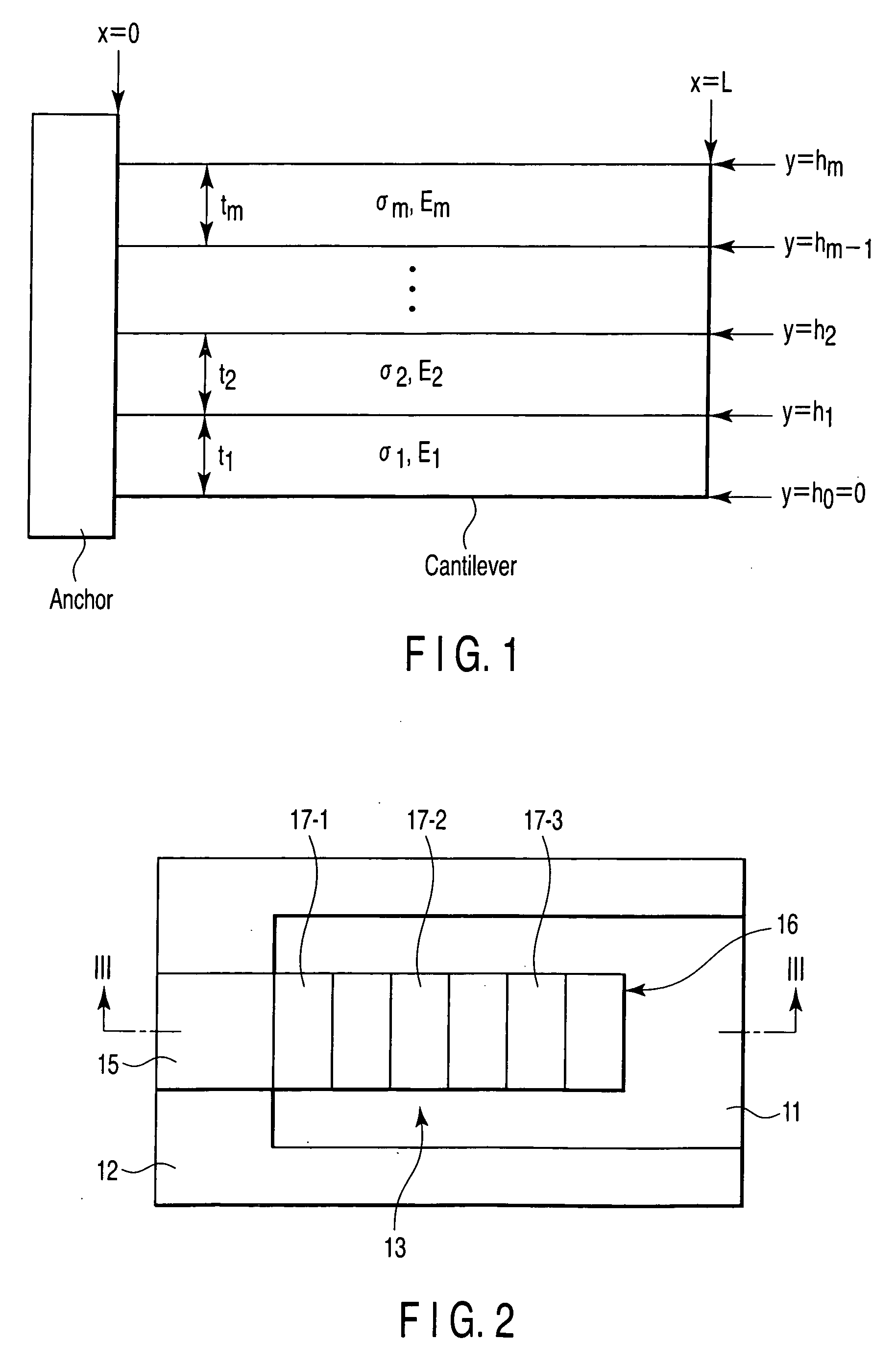
[0055] The warpage (i.e. amount of a warp) of a beam is first explained. FIG. 1 is a cross-sectional view for explaining a warp of a cantilever that is composed of a plurality of layers.
[0056] A cantilever (or a beam), which is composed of an m-number of layers, is provided on a side surface of an anchor. Specifically, the cantilever is provided over a cavity. The plural layers of the cantilever have residual stress (also referred to as “internal stress”). If two layers having different residual stresses are stacked, a stress gradient occurs in the thickness direction of the layers. Similarly, a warp occurs due to the stress gradient in the cantilever that comprises the plural layers. In the description below, the stress gradient refers to a stress gradient in the film thickness direction.
[0057] As is shown in FIG. 1, in the case where the film thickness, residual stress and Young's modulus of an i-th (i=1, 2, . . . , m) layer are ti, σi and Ei, respectively, a warp with a radius ...
second embodiment
[0109] As described above, that the warp can be adjusted by the dense / non-dense formation of concave / convex portions means that the degree of freedom for adjustment of the warp is increased. Taking advantage of this, the height of the cantilever can be adjusted. In a second embodiment of the invention, the height of the cantilever is adjusted by making use of the concave portions or convex portions that form the cantilever.
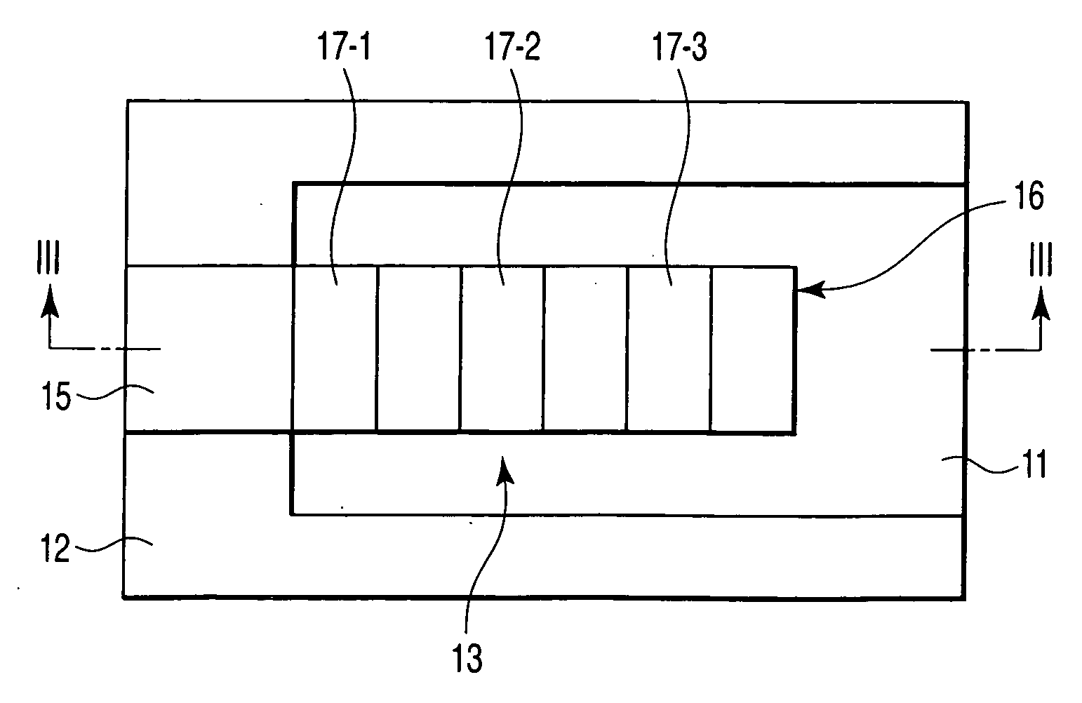
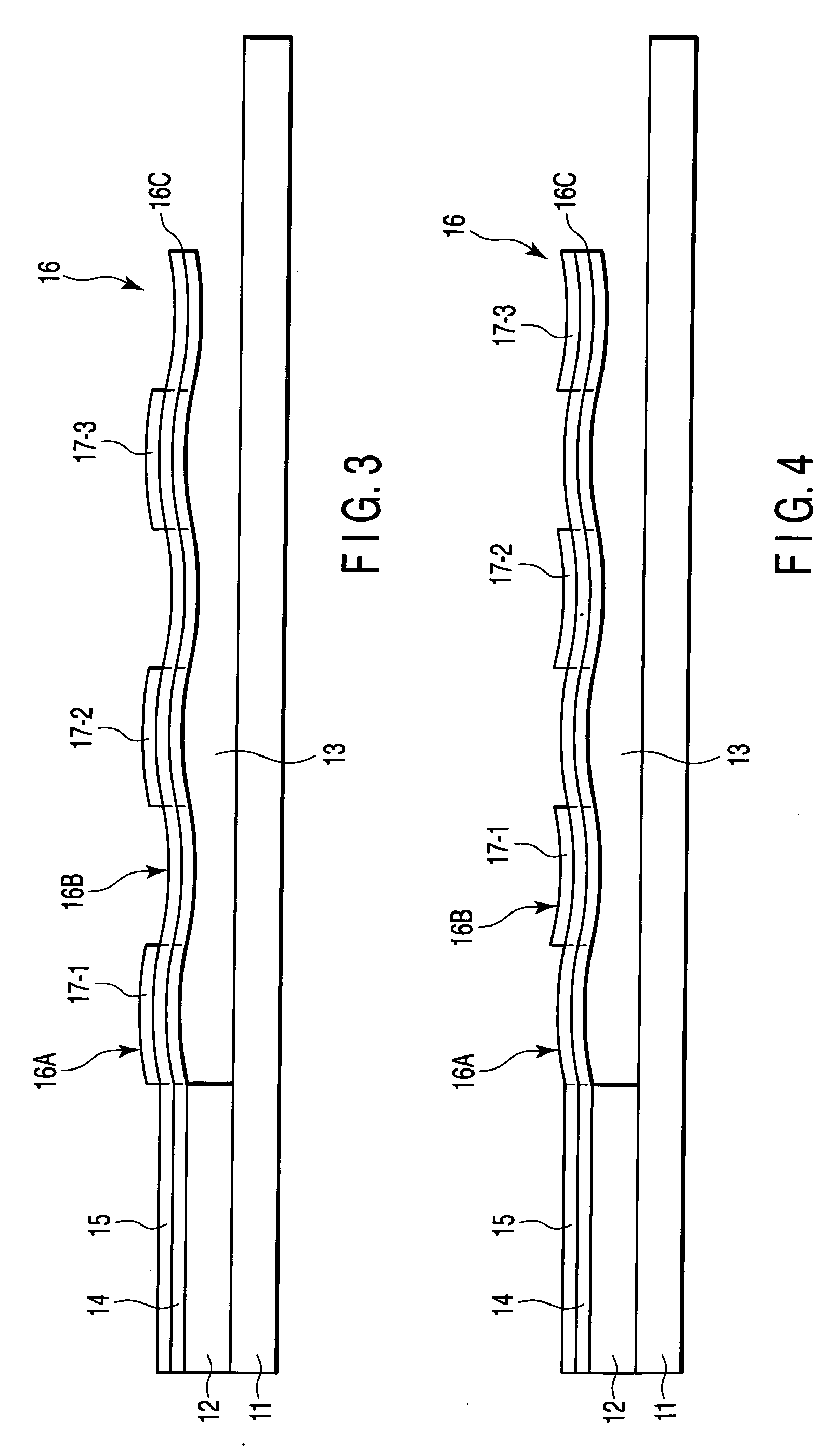
[0110]FIG. 17 is a plan view of a device comprising a cantilever according to the second embodiment of the invention. FIG. 18 is a cross-sectional view of the device, taken along line XVIII-XVIII in FIG. 17.
[0111] A cantilever 16 is provided over an anchor 12 and a cavity 13. The cantilever 16 includes a beam portion 16C and a plurality of adjustment layers 17 and 18 which are provided partly on the beam portion 16C. In addition, the cantilever 16 is composed of a base portion 16G that extends in the X-direction and a support portion 16D that supports the base p...
third embodiment
[0118] An actuator, in usual cases, is formed by stacking a plurality of layers. The actuator is a device for converting energy, such as electrical energy or chemical energy, to dynamical kinetic energy, thus performing a mechanical work. A third embodiment of the invention relates to an example in which the present invention is applied to a piezoelectric type actuator.
[0119]FIG. 19 is a plan view of a semiconductor device according to the third embodiment of the invention. FIG. 20 is a cross-sectional view of the semiconductor device, taken along line XX-XX in FIG. 19.
[0120] An anchor 12 is provided on a substrate 11. A semiconductor substrate, for instance, is used as the substrate 11. Examples of the material of the semiconductor substrate include an intrinsic semiconductor such as Si or Ge, a compound semiconductor such as GaAs or ZnSe, and a high-conductivity semiconductor which is obtained by doping impurities in these semiconductors. The semiconductor substrate may be an SO...
PUM
 Abstract
Description
Claims
Application Information