Power supply circuit
a power supply circuit and circuit technology, applied in the direction of instruments, instruments, amplifiers with semiconductor devices/discharge tubes, etc., can solve the problems of reduced phase allowance, increased current of output transistors, and difficulty in ensuring phase stability, so as to prevent the increase of chip area and the effect of consumed curren
- Summary
- Abstract
- Description
- Claims
- Application Information
AI Technical Summary
Benefits of technology
Problems solved by technology
Method used
Image
Examples
embodiment 1
Preferred Embodiment 1
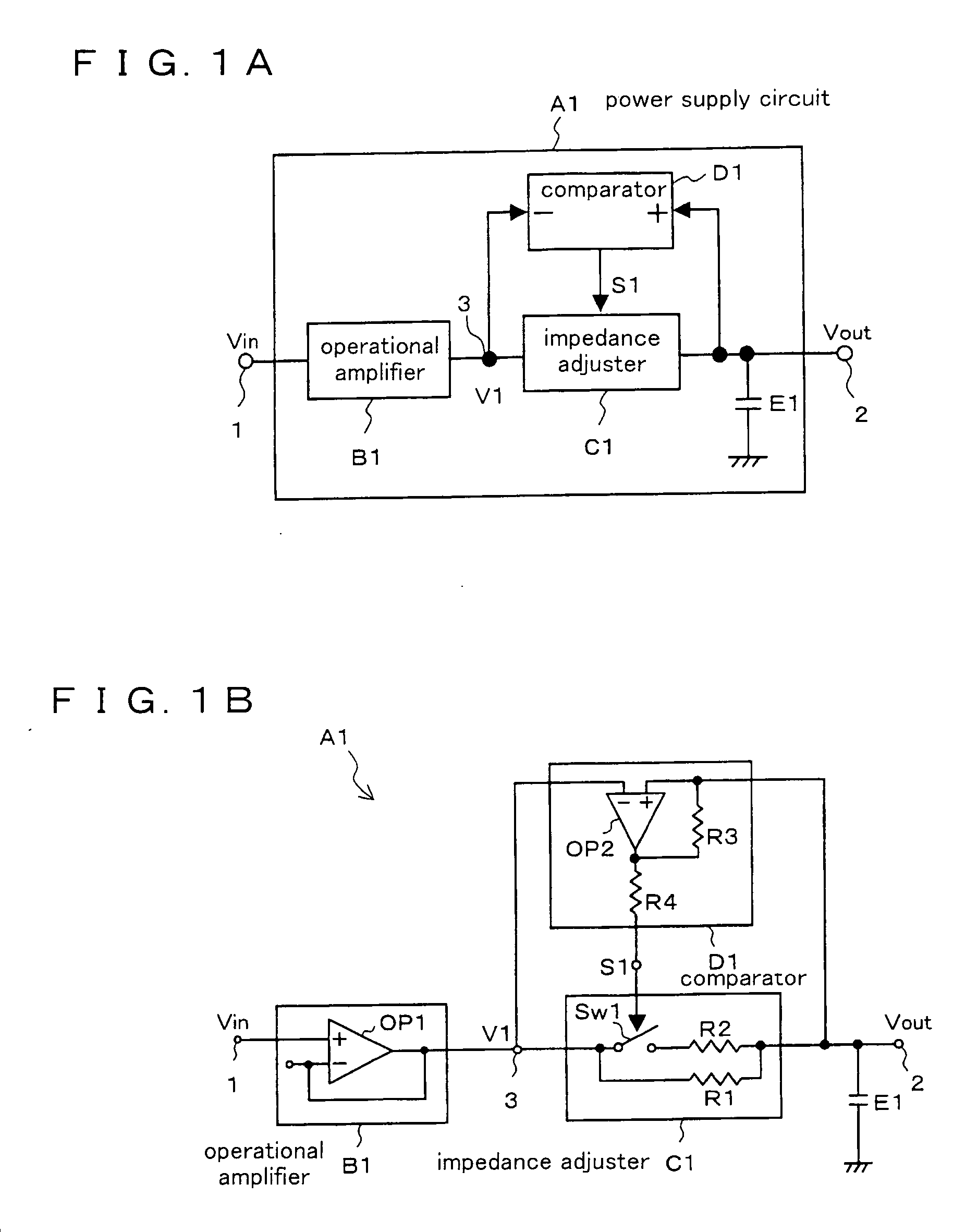
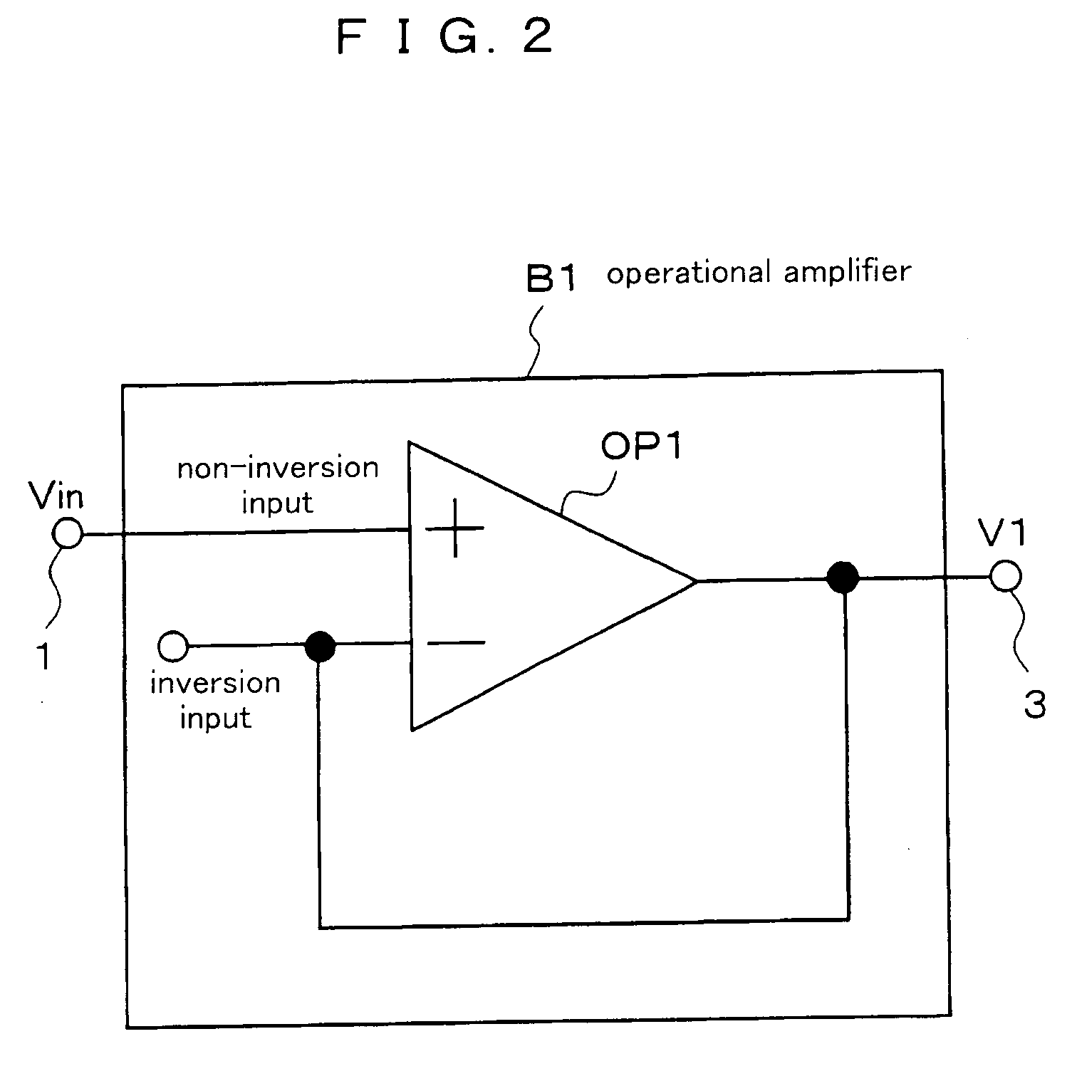
[0296] A power supply circuit according to a preferred embodiment 1 of the present invention is described below. FIG. 1A is a block diagram illustrating a constitution of the power supply circuit according to the preferred embodiment 1. FIG. 1B shows a detailed configuration of the circuit shown in FIG. 1A. Referring to reference symbols shown in FIGS. 1A and 1B, A1 denotes a power supply circuit, 1 denotes an input terminal of a reference potential Vin, 2 denotes an output terminal of the power supply circuit A1, B1 denotes an operational amplifier for generating a power supply potential V1 based on the applied reference potential Vin, C1 denotes an impedance adjuster inserted between an output terminal 3 of the operational amplifier B1 and the power supply circuit output terminal 2 and adjusting an impedance in accordance with a control signal S1, D1 denotes a comparator for comparing a power supply circuit output voltage Vout in the power supply circuit outp...
embodiment 2
Preferred Embodiment 2
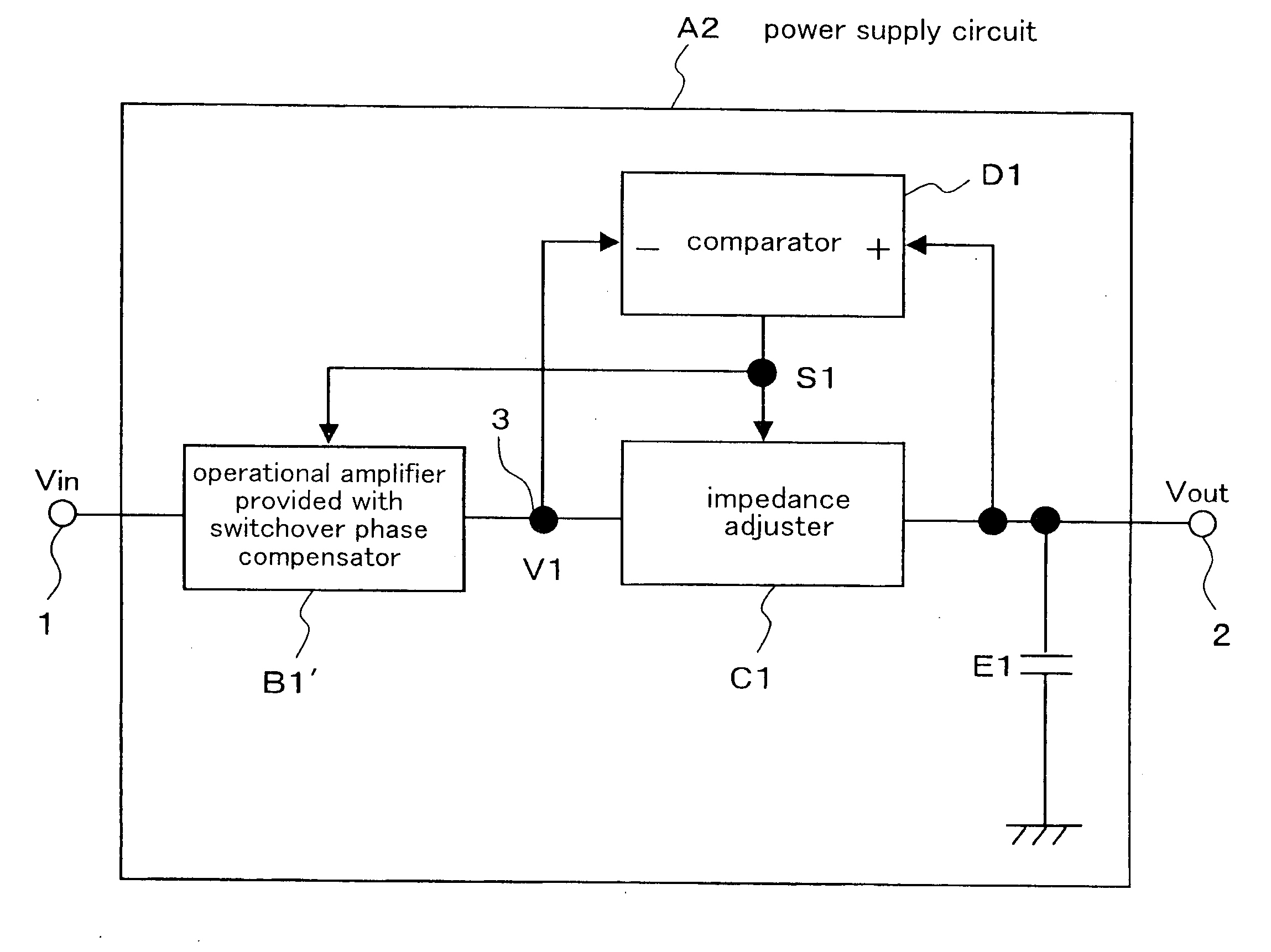
[0310]FIG. 11 is a block diagram illustrating a constitution of a power supply circuit A2 according to a preferred embodiment 2 of the present invention. In FIG. 11, the same references as those shown in FIG. 1 according to the preferred embodiment 1 denote the same constituent elements, and they are not described again. The power supply circuit A2 is provided with an operational amplifier B1′ to which a switchover phase compensator is attached in place of the operational amplifier B1. Accordingly, the impedance adjuster C1 and the operational amplifier B1′ are controlled by the control signal S1 from the comparator D1.
[0311] The operational amplifier B1′ is configured as shown in FIG. 12. A switchover phase compensator F1 is provided between the inversion input terminal (−) of the operational amplifier OP1 and an output terminal 3 of the operational amplifier B1′, and the two phase compensating circuits are selected by the switch. The operational amplifier OP...
embodiment 3
Preferred Embodiment 3
[0321]FIG. 16 is a block diagram illustrating a constitution of a power supply circuit A3 according to a preferred embodiment 3 of the present invention. In FIG. 11, the same references as those shown in FIG. 1 according to the preferred embodiment 1 denote the same constituent elements, and they are not described again. In the power supply circuit A3 according to the present preferred embodiment, the comparator D1 compares the power supply circuit output voltage Vout and the reference potential Vin applied to the input terminal 1 to each other, and outputs the control signal S1 in accordance with a result of the comparison to the impedance adjuster C1.
[0322] Accorcding to the present preferred embodiment, the input from the comparator D1 to the inversion input terminal (−) is free of any influence of the operational amplifier B1, which improves the response speed of the comparator D1. Any other operation is similar to that of the preferred embodiment 1 and is...
PUM
 Abstract
Description
Claims
Application Information


