Optical transmission device and optical phase modulator

a transmission device and optical phase technology, applied in the direction of logic circuits, instruments, pulse techniques, etc., can solve the problems of increasing the pulse width, imposing limitations on transmission rate and distance, and reducing the transmission rate and transmission distance. , to achieve the effect of facilitating the implementation of features and increasing the transmission rate and transmission distan

Inactive Publication Date: 2007-06-21
FUJITSU LTD
View PDF2 Cites 5 Cited by
  • Summary
  • Abstract
  • Description
  • Claims
  • Application Information

AI Technical Summary

Benefits of technology

[0031] Accordingly, the optical transmission device and the optical phase modulator according to an embodiment of the present invention can realize further increases in transmission rate and transmission distance, compared with the above-mentioned IM / DD technique and the technique disclosed in Japanese Unexamined Patent Application Publication No. 10-112688, as will be hereinafter described with reference to FIG. 10.
[0032] Moreover, the optical phase modulator according to the present invention requires only half the amount of the modulation bandwidth used by the known techniques. This facilitates implementation of features of known phase modulators.

Problems solved by technology

However, the wavelength dispersion characteristics of single-mode optical fibers result in an increased pulse width, degradation of the received optical signal, and interference between symbols, thereby imposing limitations on transmission rate and distance.
However, the above duo binary technique needs a signal generation procedure for converting a binary signal into a ternary signal and for obtaining a ternary electric signal for driving an optical modulator, resulting in further needs for complicated modulating means and means for driving the modulating means.
However, in signal timing 4 and signal timing 7, the phases of the CW optical signal elements in each timing are identical, or π radians, leaving the cancellation of the interference insufficient.
This phenomenon has imposed a limitation on increases in transmission rate and distance.
As a transmission distance increases, a receiving level for an optical signal becomes lower, making transmission vulnerable to interference between symbols.

Method used


Image

  • Optical transmission device and optical phase modulator
  • Optical transmission device and optical phase modulator
  • Optical transmission device and optical phase modulator

Examples


first embodiment

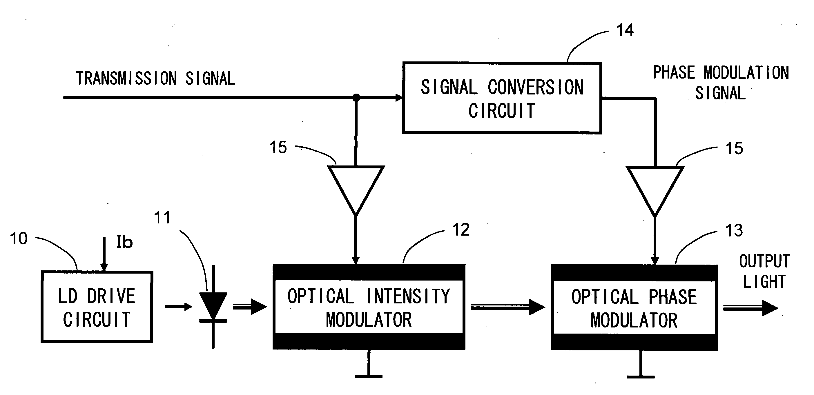
[0055]FIG. 1 is a first diagram illustrating an optical transmission device according to an embodiment of the present invention. The optical transmission device is provided with the following components: a laser diode (LD) drive circuit 10, an LD 11, an optical intensity modulator 12, an optical phase modulator 13, a signal conversion circuit 14, and plural drivers 15. The LD 11 and the optical intensity modulator 12 are coupled through an optical path. The optical intensity modulator 12 and the optical phase modulator 13 are also coupled through an optical path. The LD drive circuit 10 applies an LD current in which a bias current (Ib) is provided. The LD 11 oscillates in response to the bias current set to be larger than or equal to a stimulated emission threshold LD current and then generates a continuous wave (CW) as a source of an optical carrier signal. The optical intensity modulator 12 modulates the intensity of the CW optical signal which is generated from the LD 11 in acco...

second embodiment

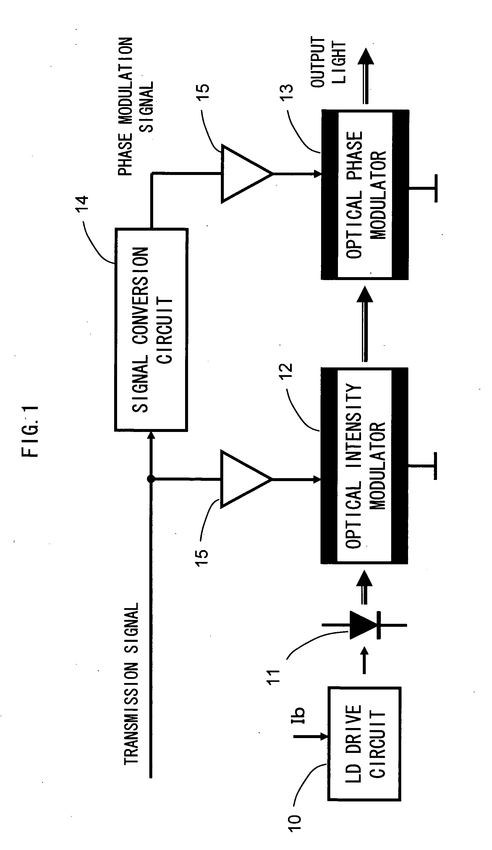
[0056]FIG. 2 is a second diagram illustrating an optical transmission device according to an embodiment of the present invention. The optical transmission device has an LD drive circuit 20 and an LD 11 which is coupled with an optical phase modulator 13 through an optical path. The LD drive circuit 20 applies to the LD 11 an LD drive current in which a bias current (Ib) and a modulation current (Ip) based on a transmission signal are provided. The LD 11 oscillates in response to the bias current (Ib) set to be larger than or equal to a stimulated emission threshold LD current. The LD 11 then generates a continuous wave (CW) as the source of an optical carrier signal which is directly modulated, so that the optical signal is in a non-luminescent state when the transmission signal is at logic level “0”, and the optical signal is in a luminescent state when the transmission signal is at logic level “1”. The optical phase modulator 13 modulates the phase of the intensity-modulated CW op...

third embodiment

[0059]FIG. 3 is a first diagram illustrating a condition in the optical phase modulator of FIG. 1 or FIG. 2. For example, in signal timing 0 to signal timing 9, a logic level sequence of a transmission signal over ten time slots is “0101100110”. In this condition, every time at least one optical signal element representing a non-luminescent state is located between optical signal elements each representing a luminescent state, the phases of the optical signal elements each representing the luminescent state are inverted with respect to each other.

[0060] In signal timing 0, output light is in the non-luminescent state, and a phase modulation signal is at logic level “1”. Thus, the phase of the output light is “π” in this timing. In signal timing 1, the output light is in the luminescent state. In this case, since the output light in the preceding timing is in the non-luminescent state, the phase is inverted to “0”. In signal timing 2, since the output light is in the non-luminescent...


PUM

PropertyMeasurementUnit
transmission distanceaaaaaaaaaa
luminescent stateaaaaaaaaaa

Abstract

An optical transmission device includes an optical phase modulator and a signal generation function. The optical phase modulator is controlled, so that when the state of an intensity-modulated optical signal shifts from a first luminescent state, through a non-luminescent state, to a second luminescent state, the phase of the optical signal in the first luminescent state and the phase of the optical signal in the second luminescent state are inverted with respect to each other, or so that when the state of the intensity-modulated optical signal shifts from the first luminescent state, through two or more non-luminescent states, to a third luminescent state, the phase of the optical signal in the first luminescent state and the phase of the optical signal in the third luminescent state are inverted with respect to each other.

Description

BACKGROUND OF THE INVENTION [0001] 1. Field of the Invention [0002] The present invention relates to an optical transmission device and an optical phase modulator for enabling increased transmission rate and transmission distance. [0003] 2. Description of the Related Art [0004] Recently, large capacity transmission networks using light have been widely used. In an optical transmission system which constitutes such an optical network, an IM / DD (intensity modulation / direct detection) scheme is extensively implemented. In such an IM / DD scheme, intensity of an optical output is modulated, using logic levels of a signal to be transmitted such as “0” and “1” which correspond to states of the optical output such as a “luminescent state” and a “non-luminescent state”, respectively. Then, the received modulated optical signal is photoelectrically converted and directly detected using a photodiode (PD) or the like. As an optical transmission line for use in the optical network, a single-mode ...

Claims


Application Information

Patent Timeline
Patent Type & Authority Applications(United States)
IPC IPC(8): G02B26/00H04B10/40G02F1/01H04B10/50H04B10/516H04B10/524H04B10/54H04B10/556H04B10/588H04B10/60H04B10/61
CPCG02F2201/16H04B10/505H04B10/5051H04B10/5055H04B10/5161H04B10/541H04B10/5561
Inventor TSUNODA, YUKITO
Owner FUJITSU LTD
Why Eureka
Try Eureka