Reconfigurable integrated circuit

a technology of integrated circuits and integrated circuits, applied in the direction of specific program execution arrangements, program control, sustainable buildings, etc., can solve the problems of increasing the difficulty of selecting the right functionality-cost mix, increasing the requirement of end customers for more sophisticated feature sets, and requiring an enormous amount of additional processing power

Inactive Publication Date: 2007-06-21
AKYA HLDG
View PDF5 Cites 288 Cited by
  • Summary
  • Abstract
  • Description
  • Claims
  • Application Information

AI Technical Summary

Benefits of technology

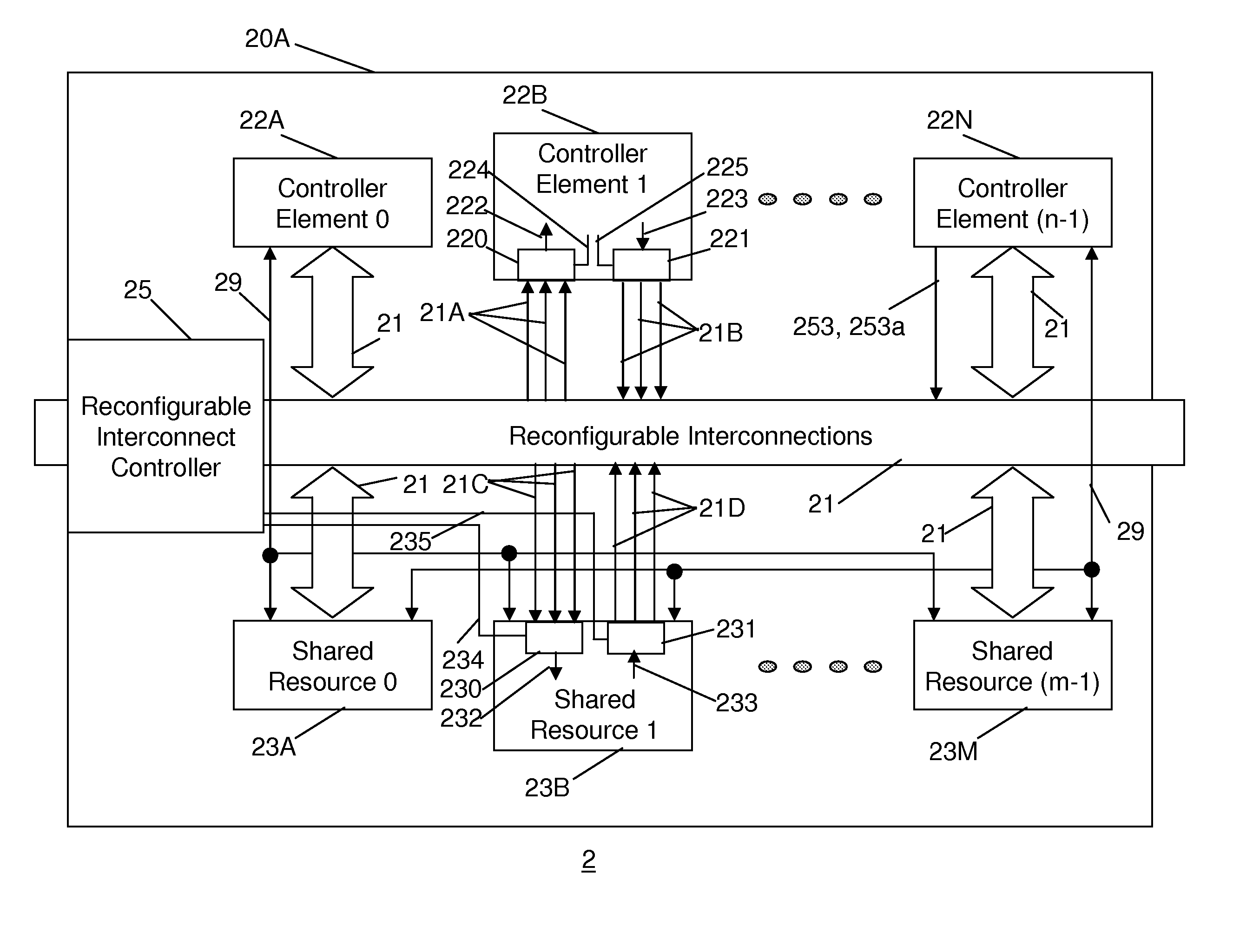
[0027] The present invention provides a reconfigurable integrated circuit comprising a plurality of controller elements, the plurality of controller elements including a first controller element and a second controller element, the first controller element having a certain architecture and a second controller element having a certain architecture, the first architecture being different from the second architecture; a plurality of processing elements, the plurality of processing elements including a first processing element and a second processing element, the first processing element having a certain architecture and a second processing element having a certain architecture, the first architecture being different from the second architecture. Reconfigurable interconnection means is used to connect and transfer data and control signals between processing elements. It is also used to interconnect processing elements and controller elements. The reconfigurable interconnection means can be dynamically reconfigured in real time and non real time providing different interconnection configurations between processing element and controller element. One or plurality of the controller elements can control the reconfigurable interconnect and implement different interconnection configurations both on a local block basis or inter-block basis.

Problems solved by technology

Functional integration, dramatic increases in complexity, new technologies and every changing and competing standards together with increased time to market pressures are making the selection of the right functionality-cost mix ever more difficult.
Furthermore, end customers are demanding more sophisticated feature sets, which in turn require an enormous amount of additional processing power.
The constant introduction of new standards means conventional equipment is effectively obsolete before it leaves the factory.
Consequently, the introduction of new equipment erodes their profits.
At the IC device level, it is becoming increasing difficult with existing IC technologies and design methodologies for designers to meet the demands outlined above.
Several IC technologies exist, but they all have disadvantages and are not optimised for a particular application.
Application Specific Integrated Circuits (ASICs) have their circuits and hence their functionality fixed at manufacture and so can't be used for new or different applications.
They have long development cycles and require huge upfront Non-Recurring Engineering (NRE) costs.
This makes them prohibitively expensive, especially for lower cost applications.
However, these devices still employ fixed or rigid hardware and as they are general purpose devices are not optimised to a particular application.
A microprocessor can only process one instruction at a time and is therefore much slower and inefficient.
While operating, many of their circuits are not being utilized.
This is a waste of expensive silicon real estate and increases power consumption.
However, this just compounds the cost, power efficiency and area issues.
However, FPGAs are very expensive and are a general-purpose device consisting of an array of uniform programmable element, usually based on look-up tables (LUTs) interconnected using programmable interconnect.
Consequently, they are not optimised for a particular application and hardware utilization can be poor.
Though they allow reconfiguration in the field the process is slow and cumbersome and doesn't allow real-time reconfiguration.
Another problem facing integrated circuit designers is the choice of device interfaces.
However, this is costly and inefficient especially when an interface requires wide address and data buses.
However, one of the problems of implementing finite state machines is that logic circuitry is required to perform functions associated with each state.
This also means these individual circuits are dissipating power even if they are not being used as in an ASIC or FPGA implementation.
For a complex state machine with many states this requires a lot of silicon resources.
One of the disadvantages of using Field Programmable Gate Arrays (FPGAs) is that they are not optimised for a particular application due to replication of uniform programmable logic elements.
However, these solutions have had many limitations.
Some have provided replicated coarse grained processing elements to target particular digital signal processing problems and therefore lack the versatility of a full reconfigurable solution.
However, the processor array is made up from the same arithmetic logic units (ALUs) repeated many times. Each ALU is 4-bits wide and control functions seem limited.
The device has specific applications and does not provide functions for implementing control, interfaces, input, output, finite state machines and general reconfiguration operations, as required in a more general purpose device.
However, this approach is limited and suffers from the disadvantages associated with ASICs and FPGAs, such as low logic utilization, greater power consumption, low speed and high cost.
However, there are several disadvantages to this approach.
This is an inefficient use of hardware resources as the computational unit controller will only be using one of the plurality of computational elements depending on the algorithm be implemented.
Therefore, the hardware utilization can be low.
Secondly, the computational unit controller can only access the computational elements in its own computation unit.
Again, this is inefficient.
Thirdly, the same computational elements and matrices are repeated across the integrated circuit to form a large array.
There are many disadvantages with this architecture.
Firstly, there is a large area overhead.
This is also a disadvantage to similar array procesors.
If it is programmed to be a memory unit, then the rest of BFU circuitry is wasted as it is not being used.
As this approach will lead to a greater silicon area and silicon costs.
Also, the logic that isn't being used directly, will probably be dissipating power.
Also, a BFU is a general purpose unit and not optimised for a particular application.
This therefore degrades the performance of the architecture and adds to the path delays.
There is also a large routing overhead associated with each BFU.
The BFUs implement many basic logic and arithmetic functions, but they are still very limited.
This is a serious disadvantage as most Digital Signal Processing (DSP) algorithms rely heavily on multiply-accumualte operations and the overall performance is degraded as it will take several clock cycles to implement a perticular function.

Method used


Image

  • Reconfigurable integrated circuit
  • Reconfigurable integrated circuit
  • Reconfigurable integrated circuit

Examples


Embodiment Construction

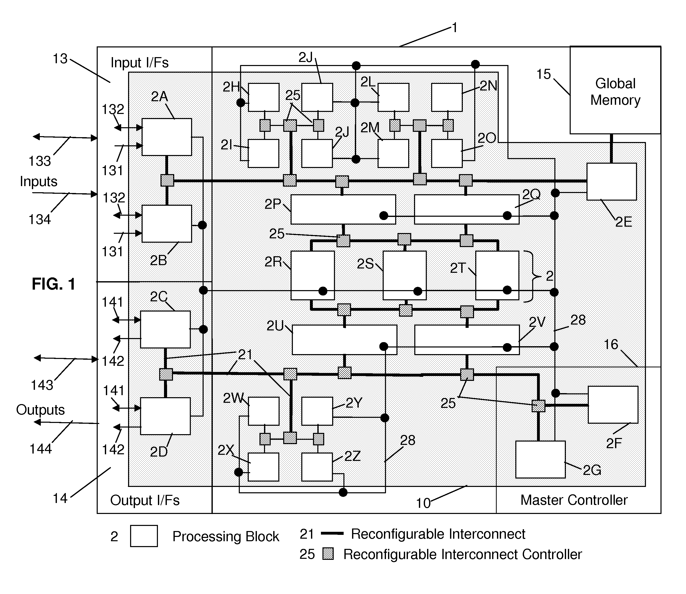
[0052]FIG. 1 shows a preferred embodiment of the present invention. The apparatus 10, referred to herein as a Reconfigurable Resource Core (“RRC”) 10, is preferably embodied as an integrated circuit 1, or as a portion of an integrated circuit having other components, such as memory 15 and or an embedded RISC core (not shown). The RRC 10 comprises one or a plurality of processing blocks 2, labelled as 2A through 2Z in FIG. 1 (individually and collectively referred to as processing blocks 2). The processing blocks 2 can communicate via reconfigurable interconnect 21. The reconfigurable interconnect 21 represents a group of buses. There is at least one bus per processing element 23 and a processing element 23 can have a plurality of output buses and individual signals. The processing element's output buses are collectively known as the reconfigurable interconnect 21. Specific routing selections are determined by the reconfigurable interconnect controllers 25. Data transferred between t...


PUM


Abstract

A reconfigurable integrated circuit is provided wherein the available hardware resources can be optimised for a particular application. Dynamically reconfiguring (in both real-time and non real-time) the available resources and sharing a plurality of processing elements with a plurality of controller elements achieve this. In a preferred embodiment the integrated circuit includes a plurality of processing blocks, which interface to a reconfigurable interconnection means. A processing block has two forms, namely a shared resource block and a dedicated resource block. Each processing block consists of one or a plurality of controller elements and a plurality of processing elements. The controller element and processing element generally comprise diverse rigid coarse and fine grained circuits and are interconnected through dedicated and reconfigurable interconnect. The processing blocks can be configured as a hierarchy of blocks and or fractal architecture.

Description

[0001] This application is a continuation-in-part of Ser. No. 10 / 685,501, filed Oct. 16, 2003, the contents of which are incorporated herein by reference.BACKGROUND OF THE INVENTION [0002] In today's competitive multimedia marketplace Integrated Circuit (IC) suppliers, Original Equipment Manufacturer (OEMs) and network / service providers are faced with an array of dilemmas. Functional integration, dramatic increases in complexity, new technologies and every changing and competing standards together with increased time to market pressures are making the selection of the right functionality-cost mix ever more difficult. Furthermore, end customers are demanding more sophisticated feature sets, which in turn require an enormous amount of additional processing power. [0003] The constant introduction of new standards means conventional equipment is effectively obsolete before it leaves the factory. This is a particular concern to network / service providers, such cable, satellite, terrestria...

Claims


Application Information

Patent Timeline
Patent Type & Authority Applications(United States)
IPC IPC(8): G06F15/00G06F15/177G06F15/78
CPCG06F15/7867H03K19/177Y02B60/1225H03K19/17756Y02B60/1207H03K19/17752Y02D10/00
Inventor SMITH, GRAEME ROY
Owner AKYA HLDG
Why Eureka
Try Eureka