Vertical type nitride semiconductor light emitting device and method of manufacturing the same

a technology of nitride and semiconductors, applied in the direction of semiconductor devices, basic electric elements, electrical equipment, etc., can solve the problems of degrading current spreading effects, disadvantageously crowded current toward a central portion, and light generated from the active layer not to be extracted, but to be absorbed into the current blocking layer with significant loss, etc., to achieve the effect of improving current spreading effects

Inactive Publication Date: 2007-06-28
SAMSUNG ELECTRONICS CO LTD
View PDF4 Cites 65 Cited by
  • Summary
  • Abstract
  • Description
  • Claims
  • Application Information

AI Technical Summary

Benefits of technology

[0012]The present invention has been made to solve the foregoing problems of the prior art and therefore an object according to certain embodiments of the present invention is to provide a nitride semiconductor light emitting device in whic...

Problems solved by technology

But this structure disadvantageously causes current to be crowded laterally, thereby degrading current spreading effects.
However, even in the vertical structure, disadvantageously current is crowded toward a central portion due to the location of the bonding metal 19b.
However this insulating mat...

Method used


Image

  • Vertical type nitride semiconductor light emitting device and method of manufacturing the same
  • Vertical type nitride semiconductor light emitting device and method of manufacturing the same
  • Vertical type nitride semiconductor light emitting device and method of manufacturing the same

Examples


Embodiment Construction

[0027]Preferred embodiments of the present invention will now be described in detail with reference to the accompanying drawings.

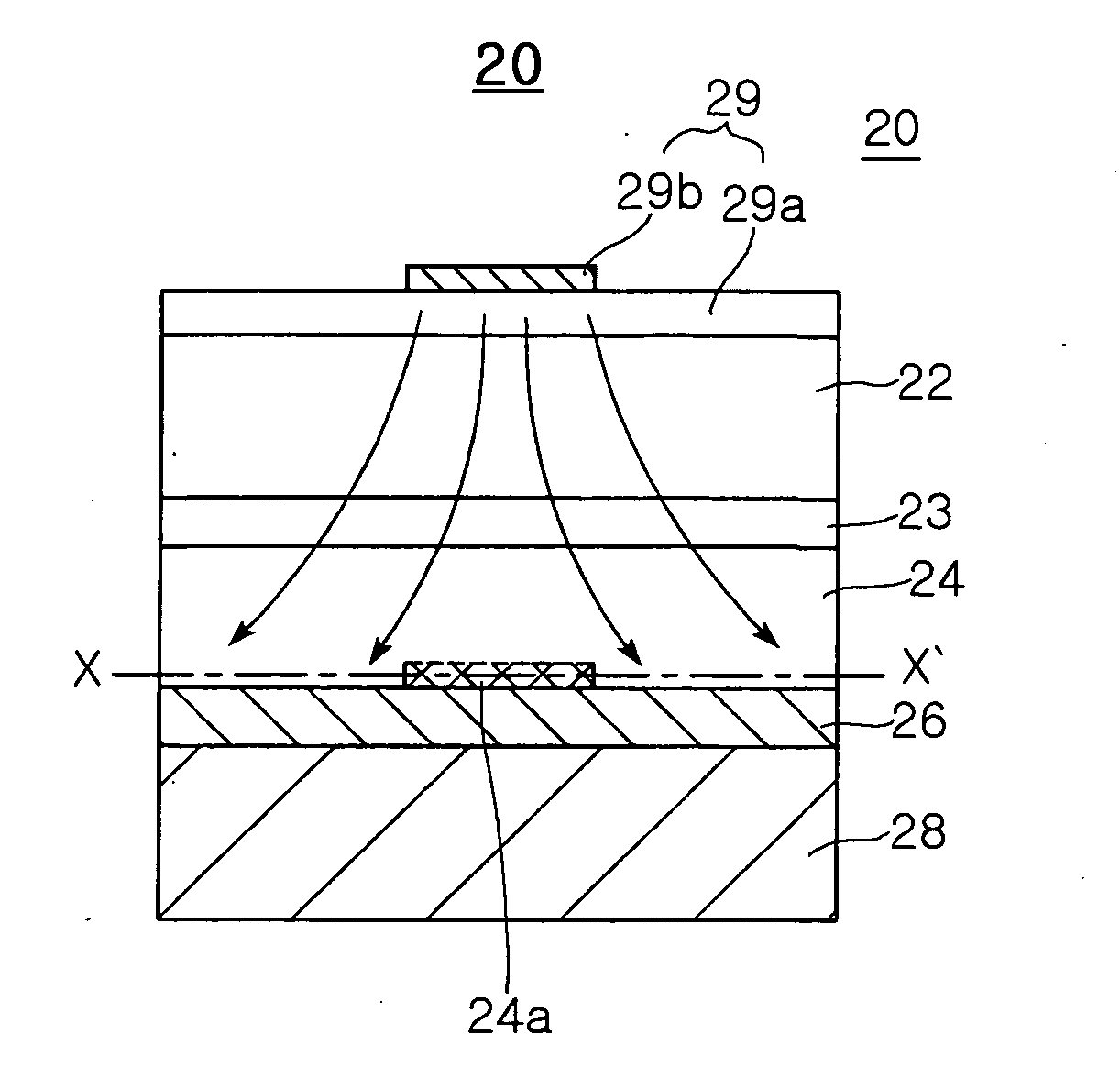
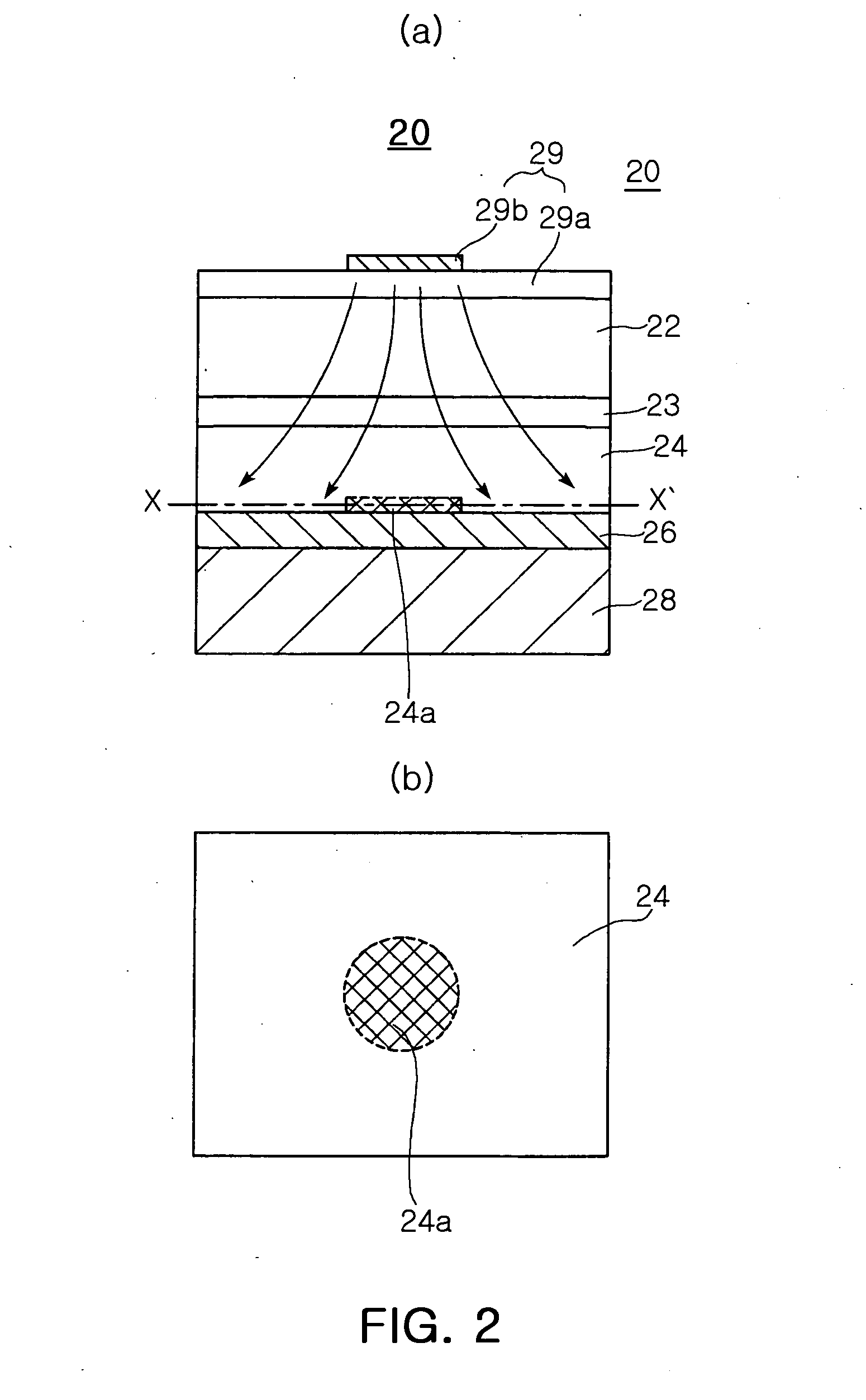
[0028]FIG. 2a is a side sectional view illustrating a vertical nitride light emitting device according to an embodiment of the invention, and FIG. 2b is a top plan view cut along the line X-X′ of FIG. 2a.

[0029]Referring to FIG. 2a, the vertical nitride light emitting device 20 according to the invention includes an ohmic contact layer 26, a p-type nitride semiconductor layer 24, an active layer 23 and an n-type nitride semiconductor layer 22 formed sequentially on a conductive substrate 28.

[0030]The conductive substrate 28 is configured as a conductive adhesive layer or separately attached via thermo-compression. Alternatively, the conductive substrate 28 may be a metal layer formed via plating. The ohmic contact layer 26 is made of a material for forming an ohmic contact with the p-type nitride semiconductor layer 24. In this embodiment, it is preferable...


PUM


Abstract

A vertical nitride semiconductor light emitting device and a manufacturing method thereof are provided. In the device, an ohmic contact layer, a p-type nitride semiconductor layer, an active layer, an n-type nitride semiconductor layer and an n-electrode are sequentially formed on a conductive substrate. At least one of a surface of the p-type nitride semiconductor layer contacting the ohmic contact layer and a surface of the n-type nitride layer contacting the n-electrode has a high resistance area of damaged nitride single crystal in a substantially central portion thereof. The high resistance area has a Schottky junction with at least one of the ohmic contact layer and the n-electrode.

Description

CLAIM OF PRIORITY[0001]This application claims the benefit of Korean Patent Application No. 2005-129350 filed on Dec. 26, 2005 in the Korean Intellectual Property Office, the disclosure of which is incorporated herein by reference.BACKGROUND OF THE INVENTION[0002]1. Field of the Invention[0003]The present invention relates to a vertical nitride light emitting device, and more particularly, to a luminescent nitride semiconductor light emitting device greatly improved in current spreading effects.[0004]2. Description of the Related Art[0005]In general, a group III-V semiconductor light emitting device is made of a semiconductor material having a composition expressed by AlxInyGa(1-x-y)N, where 0≦x≦1, 0≦y≦1 and 0≦x+y≦1. The nitride semiconductor has its crystal grown on a limited type of growth substrate such as a sapphire substrate in view of lattice constant.[0006]The sapphire substrate is electrically insulating so that the nitride semiconductor device has p- and n-electrodes formed...

Claims


Application Information

Patent Timeline
IPC IPC(8): H01L33/00H01L33/10H01L33/14H01L33/32H01L33/42
CPCH01L33/0033H01L33/145H01L33/32
Inventor BAIK, DOO GOOH, BANG WONKIM, TAE JUN
Owner SAMSUNG ELECTRONICS CO LTD
Why Eureka
Try Eureka