Pixel structure with improved charge transfer

a charge transfer and structure technology, applied in the field of pixel structures, can solve the problems of high noise level of simple passive-pixel cmos imager architecture, and inability to easily handle other analog and digital functions

Inactive Publication Date: 2007-06-28
DIERICKX BART
View PDF96 Cites 6 Cited by
  • Summary
  • Abstract
  • Description
  • Claims
  • Application Information

AI Technical Summary

Problems solved by technology

A disadvantage of CCD technology is that it cannot easily handle the other analog and digital functions that are critical on an imaging system level, such as analog to digital converters, precision amplifiers, memory, arithmetic units, and so on.
Passive pixel sensors usually make serious compromises in image quality.
Disadvantages of the simple passive-pixel CMOS imager architecture are a high noise level.
Active pixel sensors have a better noise performance than their passive pixel CMOS precursors, but typically suffer from a lower fill factor (=photosensitive portion of the pixel), and thus require a larger pixel size.
However, the image quality of pixels with CMOS-technology is still less advanced than image quality of pixels with CCD-technology.

Method used


Image

  • Pixel structure with improved charge transfer
  • Pixel structure with improved charge transfer
  • Pixel structure with improved charge transfer

Examples


Embodiment Construction

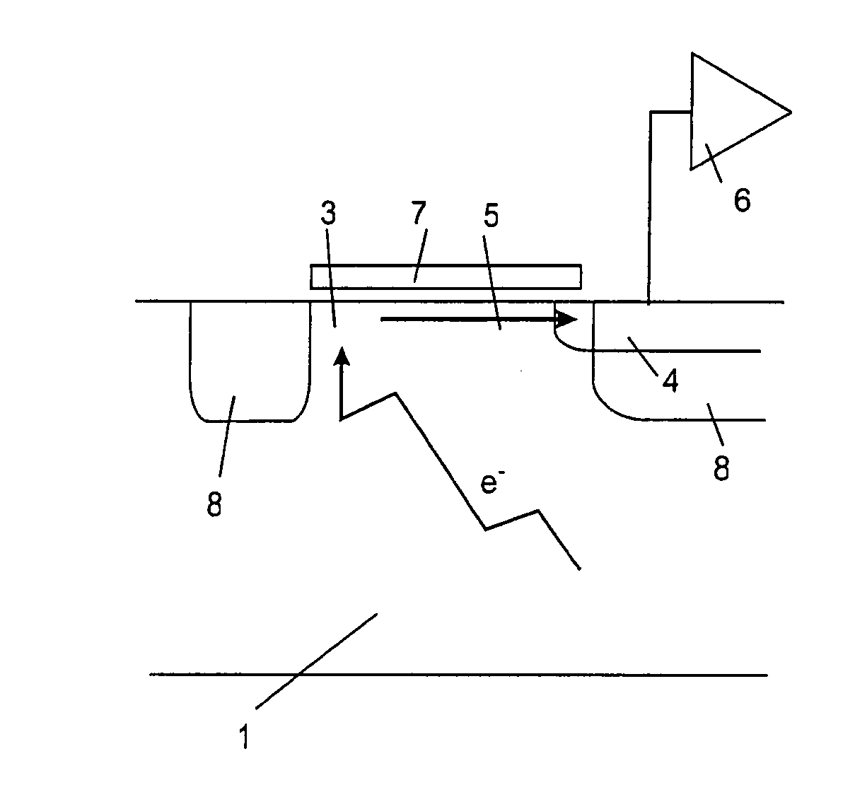
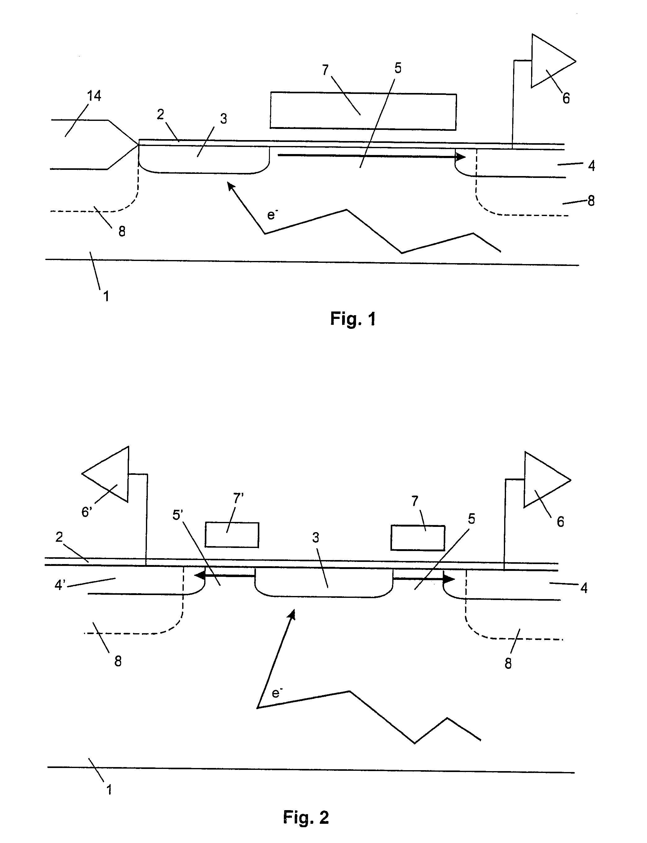
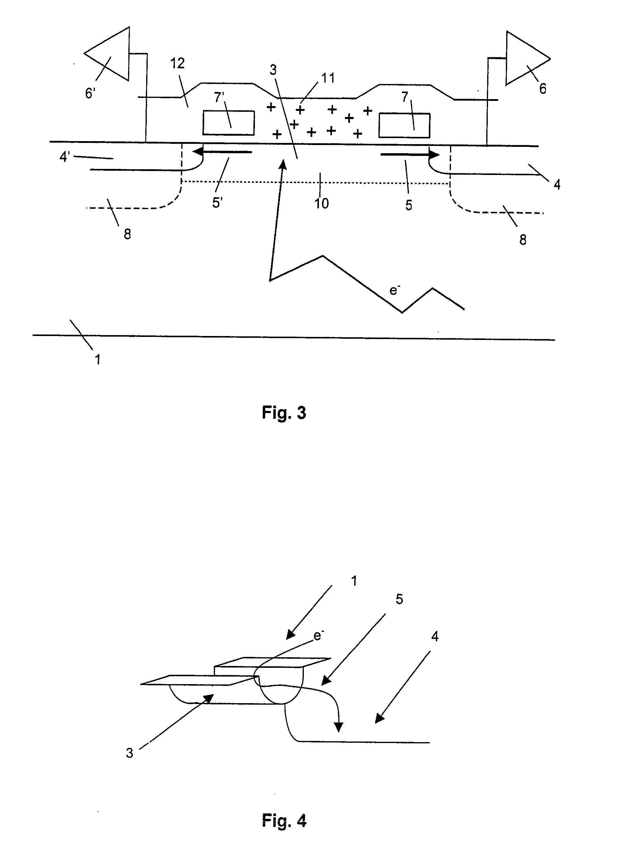
[0061] Persons skilled in the art will recognise that, in what follows, each part with as conductivity type either n-type or p-type can as well have as conductivity type respectively p-type or n-type, and that there are many values of the concentration densities which are compatible with the present invention. The word “carrier” may represent either “holes” or “electrons”. The carrier collecting region 3 and the doped or inverted region 4 are formed using techniques well understood in the art, such as diffusion and implantation. Similarly, the electrode 7 and the insulation layer 2 are formed in conventional manners.

[0062]FIG. 1 illustrates a first embodiment of a pixel structure of the present invention formed in a semiconductor substrate 1 with dopant of a first conductivity type at a first concentration density. The pixel structure may be used in an active or passive pixel. In the preferred embodiment of FIG. 1, the semiconductor substrate 1 is a p-type silicon substrate. The co...


PUM


Abstract

An active pixel is described comprising a semiconductor substrate and a radiation sensitive source of carriers in the substrate, such as for instance, a photodiode. A non-carrier storing, carrier collecting region in the substrate is provided for attracting carriers from the source as they are generated. At least one doped or inverted region of a first conductivity is provided in or on the substrate for storing the carriers before read-out. At least one non-carrier storing, planar current flow, carrier transport pathway is provided from or through the carrier collecting region to the at least one doped or inverted region to transfer the carriers without intermediate storage to the read-out electronics.

Description

BACKGROUND OF THE INVENTION [0001] The present patent application is a continuation-in-part of patent application Ser. No. 09 / 460,630, the entire contents thereof being incorporated herein by reference.TECHNICAL FIELD OF THE INVENTION [0002] The present invention relates to pixel structures such as active or passive pixel sensors and pixel arrays for detecting electromagnetic radiation using, for example, MOS-based processing technology, e.g. CMOS technology. The pixel array may be used in a camera. DESCRIPTION OF RELATED ART [0003] Commonly solid state image devices are implemented in a CCD-technology or in a CMOS or MOS technology. [0004] CCD-technology is the name of a structure of adjacent MOS gates (usually NMOS devices; PMOS CCDs (Charge Coupled Devices) are not common but have been made) that allows both storage and transport of free charge. CCD imaging is performed in a three-step process: exposure of the CCD imaging device comprising an array of pixels, charge transfer, and...

Claims


Application Information

Patent Timeline
Patent Type & Authority Applications(United States)
IPC IPC(8): H01L27/14H01L27/144H01L27/146H01L31/0352H01L31/10
CPCH01L27/1443H01L27/14603H01L27/14609H01L27/14643H01L27/14812H01L31/0352H04N3/155H04N25/585
Inventor DIERICKX, BART
Owner DIERICKX BART
Why Eureka
Try Eureka