Method of acquiring physical information and physical information acquiring device

a technology of physical information and acquiring device, which is applied in the field of acquiring physical information and acquiring physical information , can solve the problem of not being able to achieve a sufficiently reduced power consumption effect, and achieve the effect of reducing power consumption

Inactive Publication Date: 2007-06-28
SONY CORP
View PDF3 Cites 67 Cited by
  • Summary
  • Abstract
  • Description
  • Claims
  • Application Information

AI Technical Summary

Benefits of technology

[0035] However, in a case where the system disclosed in JP-A-2001-298748 is applied to a system shown in FIG. 1 in which a color processing unit 20 is disposed between a vertical signal line 18 of each column and a horizontal signal line 86, and pixel signals of a predetermined column are transmitted to an output circuit 88 through a horizontal signal line 86 by horizontal scanning using a horizontal scanning unit 12, it is not possible to achieve an effect of sufficiently reducing power consumption.

Problems solved by technology

However, in a case where the system disclosed in JP-A-2001-298748 is applied to a system shown in FIG. 1 in which a color processing unit 20 is disposed between a vertical signal line 18 of each column and a horizontal signal line 86, and pixel signals of a predetermined column are transmitted to an output circuit 88 through a horizontal signal line 86 by horizontal scanning using a horizontal scanning unit 12, it is not possible to achieve an effect of sufficiently reducing power consumption.

Method used


Image

  • Method of acquiring physical information and physical information acquiring device
  • Method of acquiring physical information and physical information acquiring device
  • Method of acquiring physical information and physical information acquiring device

Examples


first embodiment

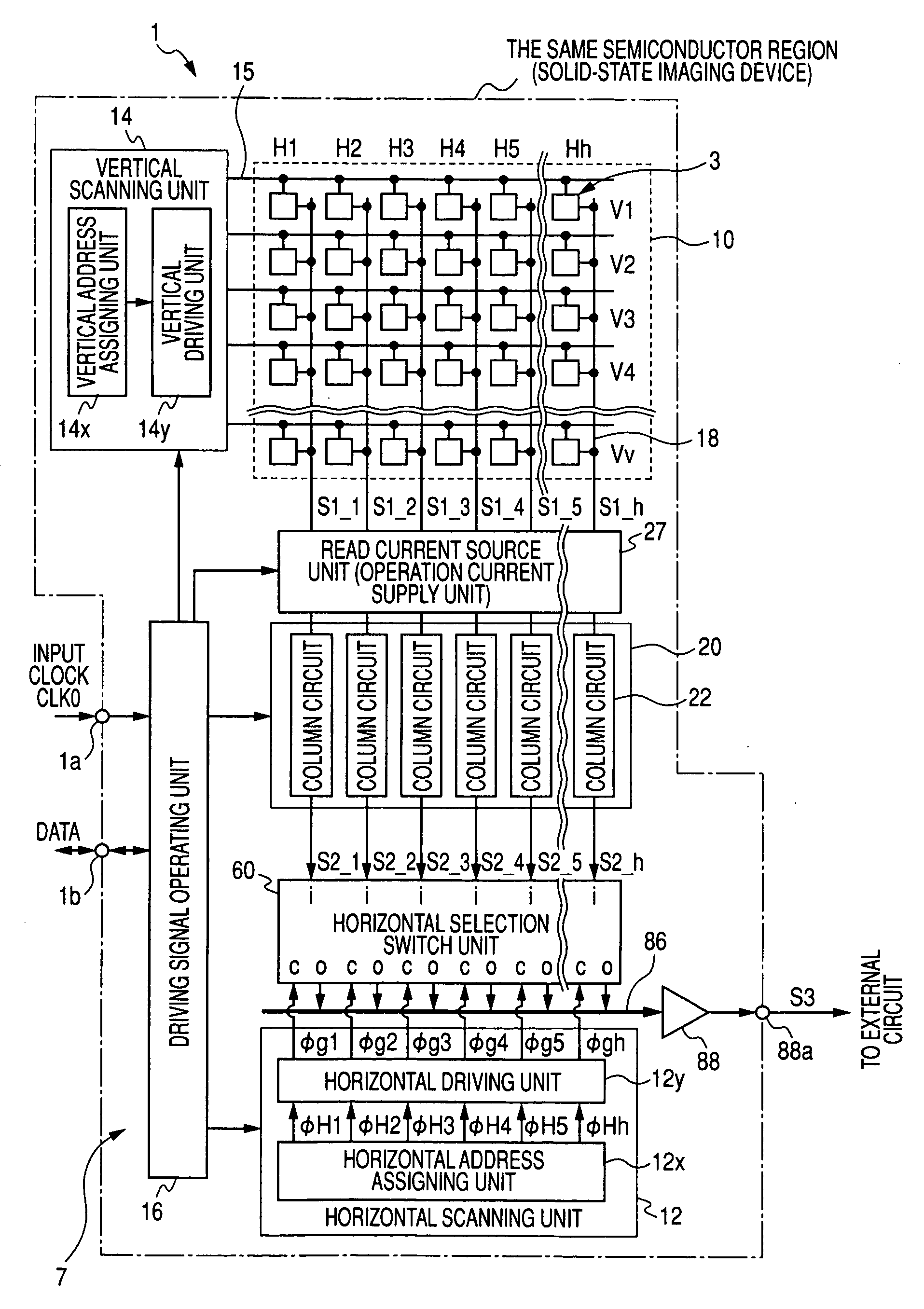
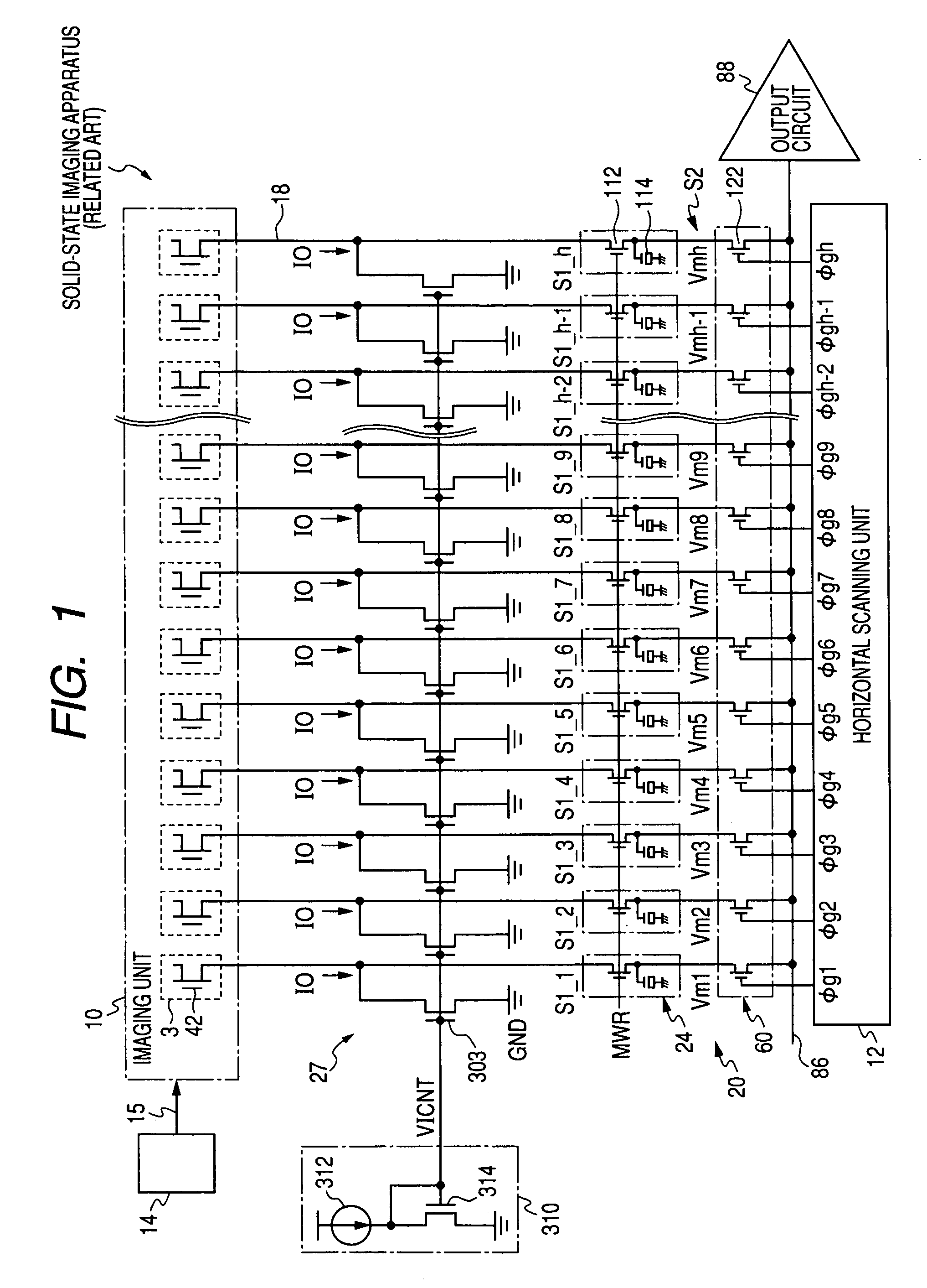
[0124]FIG. 5 is a diagram illustrating a circuit structure of a read current source unit 27 according to the invention. In FIG. 5, in addition to the read current source unit 27, a signal holding unit 24 (storage unit) that is provided as an example of a column processing unit 20, a horizontal scanning unit 12, and an output circuit 88 are shown (this is applicable to circuit structures according to the other embodiments to be described below).

[0125] According to the structure of the first embodiment, a current mirror circuit is used as a load of the source follower of the pixel signal generating unit 5, and the supply of the load current is individually controlled by the load control signal SFLACT of a plurality of systems from the load control unit 380 such that the read current source unit 27 corresponds to the combination of the thinned-out columns in the thinning-out read mode. Therefore, in the thinning-out read mode, the load current (source current) flowing through the verti...

third embodiment

[0157] Specifically, the structure may be used which allows to become zero a current flowing through the transistor 314 of the reference current source unit 310 forming the current mirror together with the current source transistors 304 of all columns. For example, in the same manner as the switch transistor 308, a switching unit, such as a semiconductor switch like the transistor, which turns on / off the current path (switches between the conductive state and the non-conductive state) may be provided between the current generating unit 312 serving as the current supply source to the transistor 314 and the transistor 314 (see a third embodiment to be described below).

[0158]

[0159]FIG. 6 is a diagram illustrating a circuit structure of a read current source unit 27 according to a second embodiment of the invention. In the structure according to the first embodiment, in a state where the current does not flow through the vertical signal line 18 of the non-read subject column from which ...

second embodiment

[0167] In this case, in order to independently control the respective switch transistors 394a and 394b by the reference voltage control signals REFCNTa and REFCENTb, the voltage stabilization control unit 398 includes a voltage stabilization control unit 398a that generates a reference voltage control signal REFCNTa for a switch transistor 394a, and a voltage stabilization control unit 398b that generates a reference voltage control signal REFCNTb for a switch transistor 394b.

[0168] As such, the individual voltage stabilization control units 398a and 398b may be provided as the hardware circuit structures. In addition, the reference voltage control signals REFCNTa and REFCNTb may be independently output by the single voltage stabilization control unit 398. This point is the same as that of the load control units 380a and 380b.

[0169] By using this structure, in the thinning-out read mode, the load control unit 380b controls the load control signal SFLACb to turn off the switch tra...


PUM


Abstract

Disclosed is a method of acquiring physical information that acquires physical information by using a semiconductor device. The semiconductor device includes unit elements, each of which has a detecting unit and a unit signal generating unit. The method includes the steps of: providing an operation current supply unit supplying an operation current such that the unit signal generating unit outputs a unit signal, and a signal processing unit receiving the unit signal output from each of the unit elements forming the semiconductor device and outputting an output unit signal; and when a selective read mode is designated for reading the unit signal from a portion of the respective unit elements, an operation current of the output signal line of the unit signal generating unit not to be read is reduced so as to be smaller than an operation current of the output signal line of the unit signal generating unit to be read.

Description

CROSS REFERENCES TO RELATED APPLICATIONS [0001] The invention contains subject matter related to Japanese Patent Application JP 2005-332871 filed in the Japanese Patent Office on Nov. 17, 2005, the entire contents of which being incorporated herein by reference. BACKGROUND OF THE INVENTION [0002] 1. Field of the Invention [0003] The present invention relates to a method of acquiring physical information and a physical information acquiring device. More particularly, the invention relates to an operation mode in which partial information is used by reducing an information amount, by using a semiconductor device for physical quantity distribution detection, such as a solid-state imaging device including an array of a plurality of unit elements sensitive to an electromagnetic wave, such as light or radiation, incident from the outside and capable of reading an electrical signal indicating a physical quantity distribution converted into the electrical signal by the unit elements. [0004]...

Claims


Application Information

Patent Timeline
Patent Type & Authority Applications(United States)
IPC IPC(8): H04N5/335H04N5/374H04N5/3745H04N5/376
CPCG11C19/282H04N5/3456H04N5/3741H04N5/3742H04N5/3765H04N5/378H04N25/445H04N25/766H04N25/767H04N25/75H04N25/745
Inventor MAEDA, NORIYAUI, HIROKINISHIZONO, SHINICHIRO
Owner SONY CORP
Why Eureka
Try Eureka