Thin film transistor device, method for manufacturing the same and display apparatus having the same

a technology of thin film transistors and transistors, which is applied in the direction of semiconductor devices, basic electric elements, electrical equipment, etc., can solve the problems of deterioration of storage capacitors, long process time, and low mass productivity of doping processes, so as to reduce the connection resistance of upper-layer electrodes through contact holes, excellent display properties, and low resistance

Inactive Publication Date: 2007-06-28
MITSUBISHI ELECTRIC CORP
View PDF1 Cites 44 Cited by
  • Summary
  • Abstract
  • Description
  • Claims
  • Application Information

AI Technical Summary

Benefits of technology

[0012]The present invention has been made in view of above circumstances and provides a TFT and a manufacturing method thereof to solve the foregoing problems caused by a thin polysilicon film serving as a conductive film which is the lowest layer of the TFT. That is, according to an embodiment of the invention, there is provided a TFT and a manufacturing method in which damage given to an insulating film by doping is suppressed to a minimum so as to secure excellent mass productivity, and the resistance of a lower electrode of a storage capacitor can be reduced easily so as to contribute to improvement in properties. According to another embodiment of the invention, there is provided a TFT and a manufacturing method to attain excellent electric conduction between a signal wire of a TFT and a doped region of a thin polysilicon film serving as the conductive film which is the lowest layer. According to a further embodiment of the invention, there is provided a TFT and a manufacturing method to reduce a total connection resistance between the doped region of the polysilicon film and a pixel electrode in which resistance has especially great influence on display.
[0014]According to the above configuration, the metal film is formed to have a portion that coats a doped region of a thin polysilicon film serving as a conductive film and that overlaps just under a contact hole. Accordingly, there is an effect that the connection resistance with an upper-layer electrode through the contact hole can be reduced, so that excellent display properties can be obtained. In addition, a lower electrode of a storage capacitor can be formed out of the metal film having low resistance. Accordingly, there is an effect that deterioration of an insulating layer caused by doping can be suppressed, and the mass productivity can be secured, while a stable capacitance can be formed so that the display properties can be improved.

Problems solved by technology

To this end, a long process time is required.
The doping process is a process with low mass productivity.
The doping inevitably leads to damage on an insulating film serving as a capacitance of the storage capacitor, causing deterioration in storage capacitor.
Further, as long as the lower electrode is formed out of the polysilicon film, there is a limit in reduction of resistance only by the concentration of the dopant.
There is a problem that the lower electrode itself has a capacitance component which resists desired properties.
In addition to the problem caused by the capacitance component, there is another problem that a resistance component in series with the storage capacitor increases due to the polysilicon film elongated to the lower electrode of the storage capacitor.
In addition, the manner in which etching is carried out in two stages to open contact holes is not suitable for mass productivity.
Further, the method in which a polysilicon film has an undercoat separately formed of another silicon film has a limited effect in view from selectivity and may not completely cope with variation in terms of the thickness of the interlayer insulating film and the in-plane distribution of the etching rate.
If an opening of a contact hole is not formed in good condition, electric conduction between a signal wire and a doped region of the polysilicon film will be insufficient, or signal transmission between the doped region of the polysilicon film and a pixel electrode portion will not be attained in good condition.
Thus, a defect on display will be brought about.

Method used


Image

  • Thin film transistor device, method for manufacturing the same and display apparatus having the same
  • Thin film transistor device, method for manufacturing the same and display apparatus having the same
  • Thin film transistor device, method for manufacturing the same and display apparatus having the same

Examples


embodiment 1

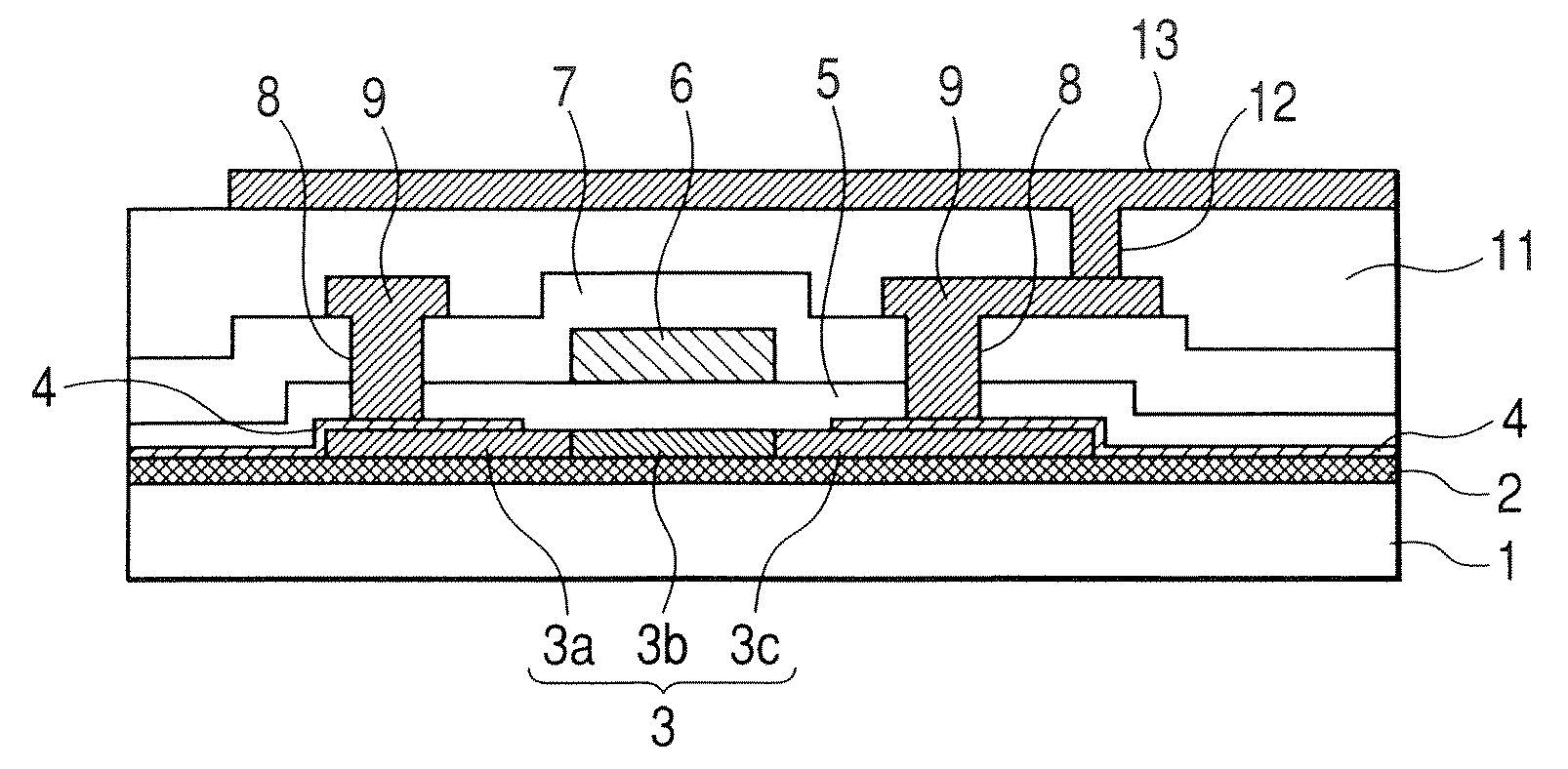
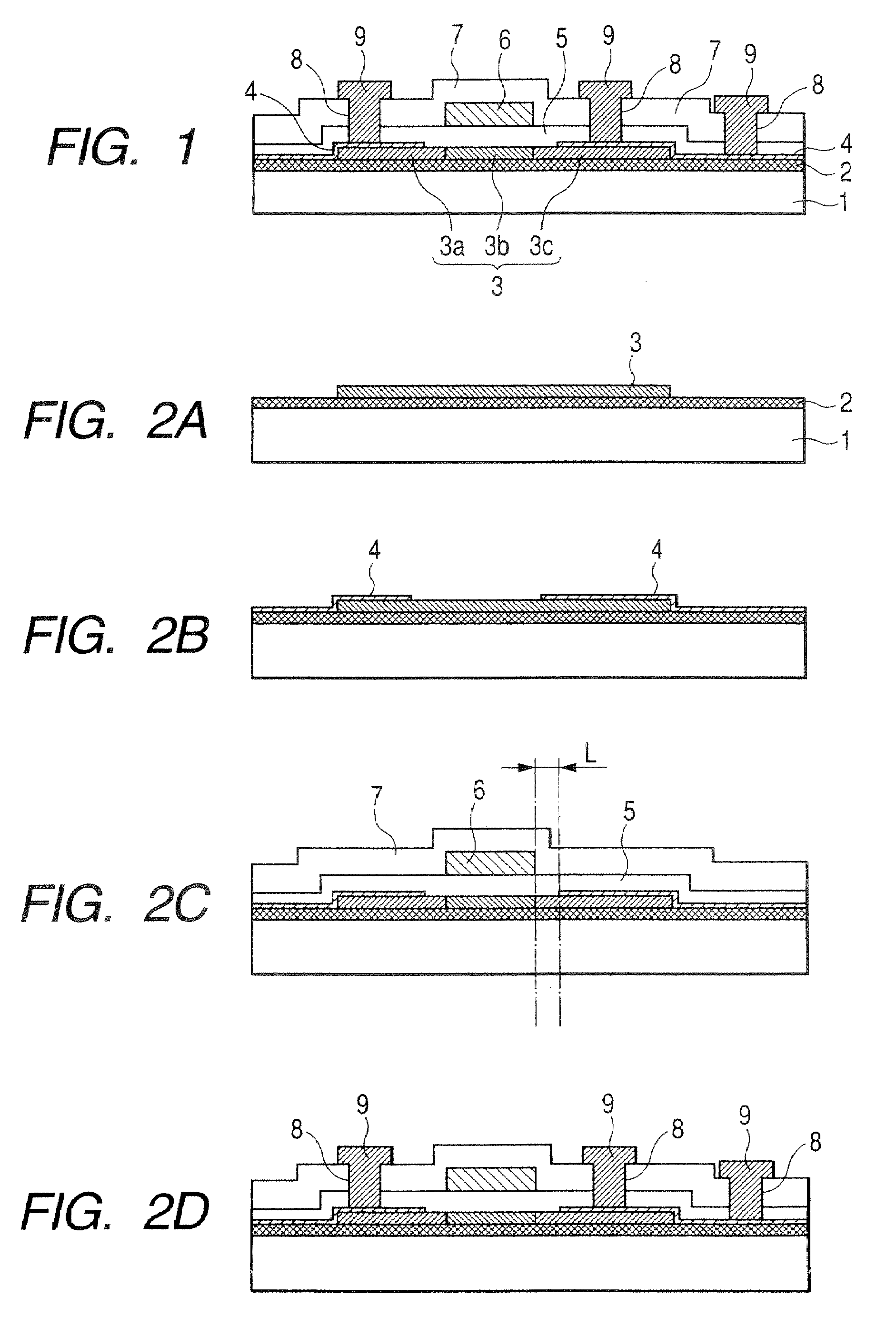
[0021]FIG. 1 shows a sectional view of a substrate for a liquid crystal panel according to Embodiment 1.

[0022]In FIG. 1, a polysilicon film 3 formed on a protective insulating film 2 on a glass substrate 1 has a source region 3a, a drain region 3c and a channel region 3b. A metal film 4 is provided to cover the source region 3a and the drain region 3c. A gate insulating film 5 is formed to cover the protective insulating film 2, the polysilicon film 3 and the metal film 4. A gate electrode 6 is formed on top of the gate insulating film 5 so as to be located above the channel region 3b. Further the gate insulating film 5 and the gate electrode 6 are coated with an interlayer insulating film 7 made of SiO2 or the like. Signal wires 9 are provided on top of the interlayer insulating film 7 so as to be connected to the metal film 4 on the source region 3a and the drain region 3c through contact holes 8 provided in the interlayer insulating film 7 and the gate insulating film 5.

[0023]In ...

embodiment 2

[0031]In Embodiment 1 of the invention, due to a metal film formed as a layer covering a thin polysilicon film, it is possible to solve one of problems caused by use of the thin polysilicon film. That is, it is possible to prevent the polysilicon film from being etched through when contact holes are opened. As a result, it is possible to suppress increase in connection resistance between a drain region and a signal wire. According to Embodiment 2 of the invention, there is provided another effect.

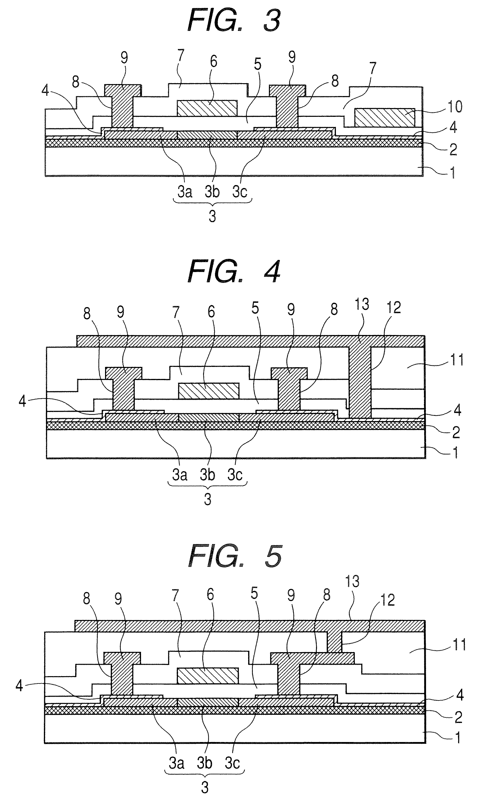
[0032]FIG. 3 shows a sectional view of a TFT device according to Embodiment 2 of the invention. In FIG. 3, constituent parts the same as those in Embodiment 1 shown in FIG. 1 are referenced correspondingly. The following points are not shown in FIG. 1. That is, there is provided an upper electrode 10 of a storage capacitor, which is formed in the same layer as the gate electrode 6, and the metal film 4 is also used as a lower electrode of the storage capacitor opposed to the upper electrode...

embodiment 3

[0036]In Embodiment 1 of the invention, due to a metal film formed as a layer covering a thin polysilicon film, it is possible to solve one of problems caused by use of the thin polysilicon film. That is, it is possible to prevent the polysilicon film from being etched through when contact holes are opened. As a result, it is possible to suppress increase in connection resistance between a drain region and a signal wire. According to Embodiment 3 of the invention, the total connection resistance between a drain region and a pixel electrode is further suppressed from increasing compared with Embodiment 1.

[0037]A TFT device according to Embodiment 3 of the invention will be described below with reference to FIG. 4. In FIG. 4, constituent parts the same as those in Embodiment 1 shown in FIG. 1 are referenced correspondingly. The following points are added to the configuration of FIG. 1. That is, an upper insulating film 11 is formed to cover the TFT shown in FIG. 1, a pixel electrode 1...


PUM


Abstract

A thin film transistor device includes: an island shaped semiconductor layer; a metal film that covers at least a part of a source region and a drain region of the semiconductor layer; a gate insulating film that covers the semiconductor layer and the metal film; an interlayer insulating film that covers the gate insulating film; and a signal wire that lies on the interlayer insulating film. The gate insulating film and the interlayer insulating film are formed with contact hole that reaches the metal film. The signal wire is connected to the metal film through the contact hole.

Description

BACKGROUND OF THE INVENTION[0001]1. Field of the Invention[0002]The present invention relates to a thin film transistor (TFT) device for use in an electro-optic display apparatus based on an active matrix system, particularly in a liquid crystal display apparatus or an organic electroluminescence (EL) type display apparatus, and a method for manufacturing the TFT device.[0003]2. Description of the Related Art[0004]In recent years, thin-profile display apparatus using TFTs, such as liquid crystal display apparatus or EL display apparatus, have been developed. Further, attention has been paid to TFTs using polysilicon as a material of an active region for the following reasons. That is, a high-definition panel can be formed as compared with a panel heretofore formed out of TFTs using amorphous silicon. A driving circuit region and a pixel region can be formed integrally. The cost of driving circuit chips or the cost of mounting the chips is dispensable. Thus, the manufacturing cost ca...

Claims


Application Information

Patent Timeline
Patent Type & Authority Applications(United States)
IPC IPC(8): H01L21/84H01L21/00
CPCH01L29/41733H01L27/124H01L27/1255H01L29/458H01L27/12H01L27/1214H01L27/13
Inventor NAGATA, HITOSHIITOH, YASUYOSHI
Owner MITSUBISHI ELECTRIC CORP
Why Eureka
Try Eureka