Metal-insulator-metal capacitor structure having low voltage dependence

a technology of metal-insulator and capacitor, which is applied in the direction of capacitor, semiconductor device, semiconductor/solid-state device details, etc., can solve the problems of large circuit area occupied by the im capacitor in such integrated circuit designs, undesirable to mixed signal, radio frequency, analog circuit,

Inactive Publication Date: 2007-07-05
TAIWAN SEMICON MFG CO LTD
View PDF15 Cites 47 Cited by
  • Summary
  • Abstract
  • Description
  • Claims
  • Application Information

AI Technical Summary

Benefits of technology

[0032] Since the semiconductor capacitor device comprises two MIM capacitors electrically connected in series and using silicon oxide and a high k dielectric material as a dual capacitor dielectric, the invention can provide increased capacitance density as does the related art. Moreover, since the dual capacitor dielectric have opposite VCC characteristics, the total VCC value can be further minimized to increase the operating voltage range of the integrated circuits using MIM capacitors. Furthermore, the semiconductor capacitor device comprising two MIM capacitors electrically connected in series can further reduce leakage current.

Problems solved by technology

MIM capacitors in such integrated circuit designs, however, may occupy a large portion of the circuit area.
This is undesirable to mixed signal, radio frequency, and analog circuits because they typically require closer capacitor matching and relatively. good voltage linearity (low voltage dependence or low VCC value).

Method used


Image

  • Metal-insulator-metal capacitor structure having low voltage dependence
  • Metal-insulator-metal capacitor structure having low voltage dependence
  • Metal-insulator-metal capacitor structure having low voltage dependence

Examples


Embodiment Construction

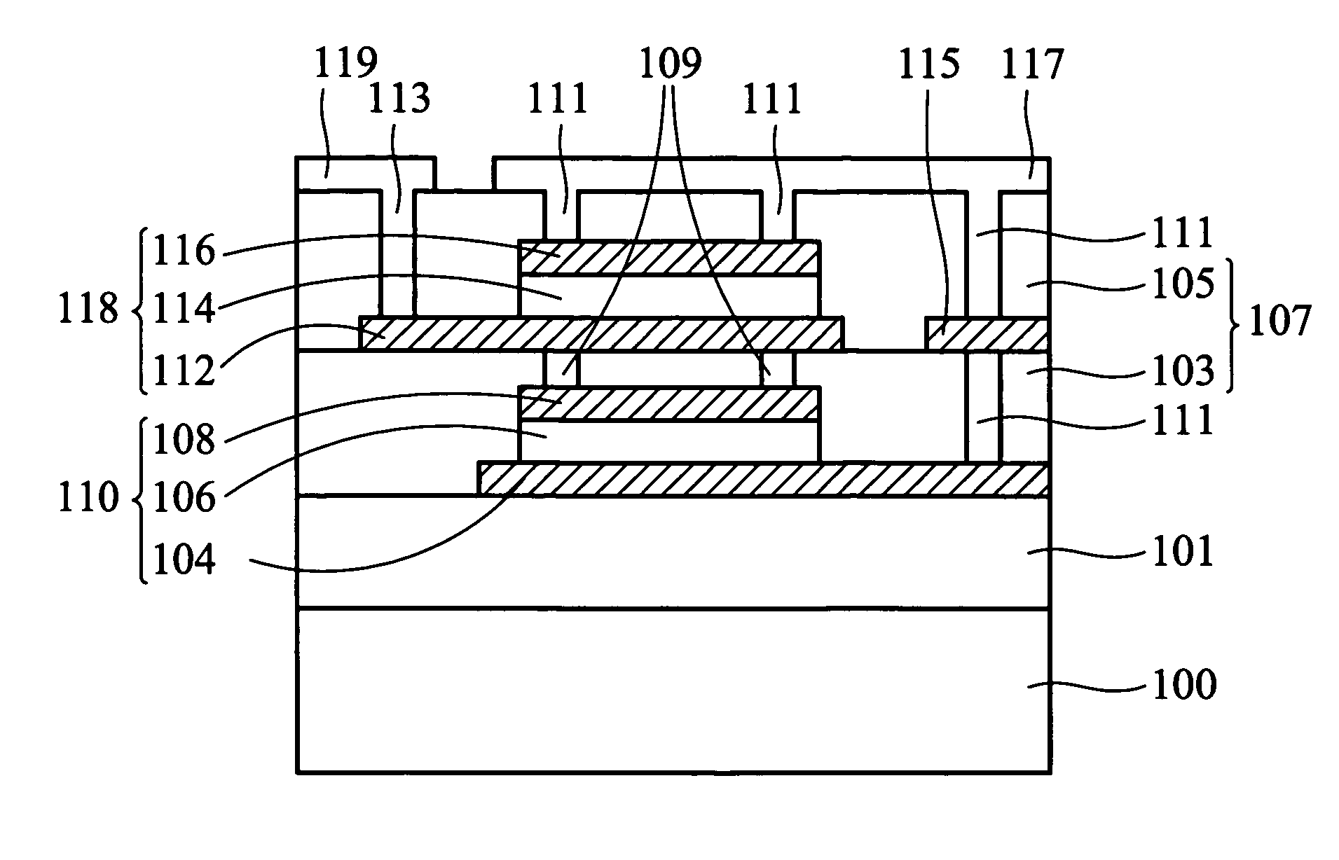
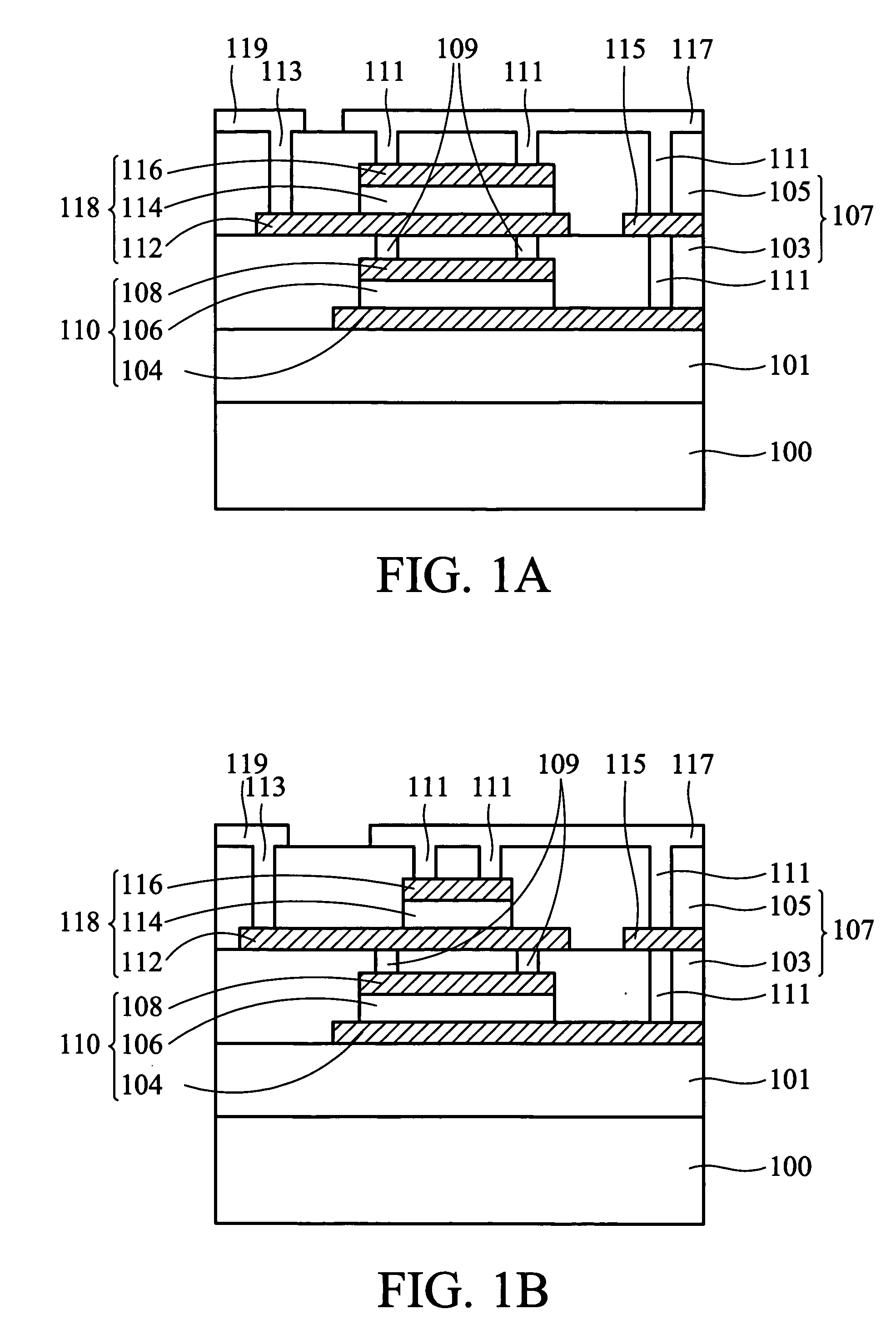
[0017] The following description is of the best-contemplated mode of carrying out the invention. This description is provided for the purpose of illustrating the general principles of the invention and should not be taken in a limiting sense. The scope of the invention is best determined by reference to the appended claims. The semiconductor capacitor device of this invention will be described below with reference to the accompanying drawings.

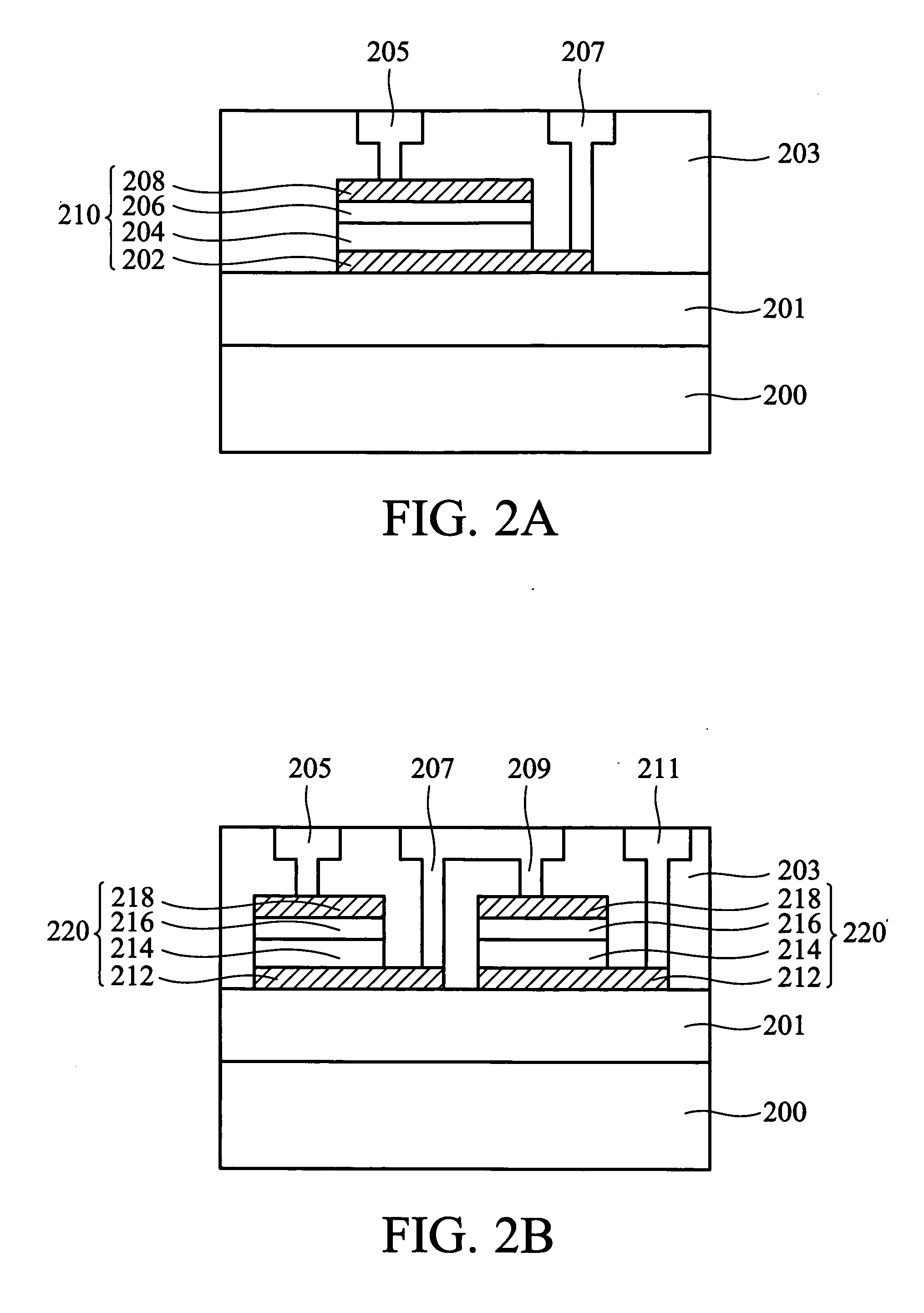
[0018] The invention relates to an improved semiconductor capacitor device for different integrated circuit designs, such as mixed signal, radio frequency, and analog circuits, thereby increasing capacitance density while keeping the VCC value low. FIG. 1A illustrates an embodiment of a semiconductor capacitor device. In FIG. 1A, a substrate 100 is provided. The substrate 100, such as a silicon substrate or other semiconductor substrates, may contain a variety of elements, including, for example, transistors, resistors, and other semiconductor...


PUM


Abstract

A semiconductor capacitor device. A dielectric layer is on a substrate. A stack capacitor structure is disposed in the dielectric layer and comprises first and overlying second MIM capacitors electrically connected in parallel. The first and second MIM capacitors have individual upper and lower electrode plates and different compositions of capacitor dielectric layers.

Description

BACKGROUND OF THE INVENTION [0001] 1. Field of the Invention [0002] The present invention relates to a semiconductor device, and in particular to a metal-insulator-metal (MIM) capacitor structure that increases capacitance density while keeping the voltage linearity coefficient (VCC) value low. [0003] 2. Description of the Related Art [0004] Reduced circuit area is an important concern in microelectronics technology. Integrated circuits continue to increase in circuit density due to the reduced size of circuit components. As more components are incorporated into an integrated circuit, higher performance in the circuit can be achieved. One type circuit component that is increasingly incorporated into integrated circuit designs, such as mixed signal, radio frequency, and analog circuits, is a metal-insulator-metal (MIM) capacitor, which typically includes a stacked arrangement of materials of upper and lower metal electrode plates and an intermediate capacitor dielectric layer. [0005]...

Claims


Application Information

Patent Timeline
Patent Type & Authority Applications(United States)
IPC IPC(8): H01L29/00
CPCH01L23/5223H01L28/60H01L2924/0002H01L2924/00
Inventor YEH, DER-CHYANGLIN, CHIE-IUANLEE, CHUAN-YINGCHAO, Y. T.CHEN, MING-HSIEN
Owner TAIWAN SEMICON MFG CO LTD
Why Eureka
Try Eureka