

Multi-Layer Printed Circuit Board and Method for Fabricating the Same
- Summary
- Abstract
- Description
- Claims
- Application Information
AI Technical Summary
Benefits of technology
Problems solved by technology
Method used
Image

Examples
Embodiment Construction
[0001]1. Field of the Invention
[0002]The present invention relates to a printed circuit board, and more particularly, to a double-sided or multi-layer printed circuit board (PCB) and method for fabricating the same.
[0003]2. Background of the Invention
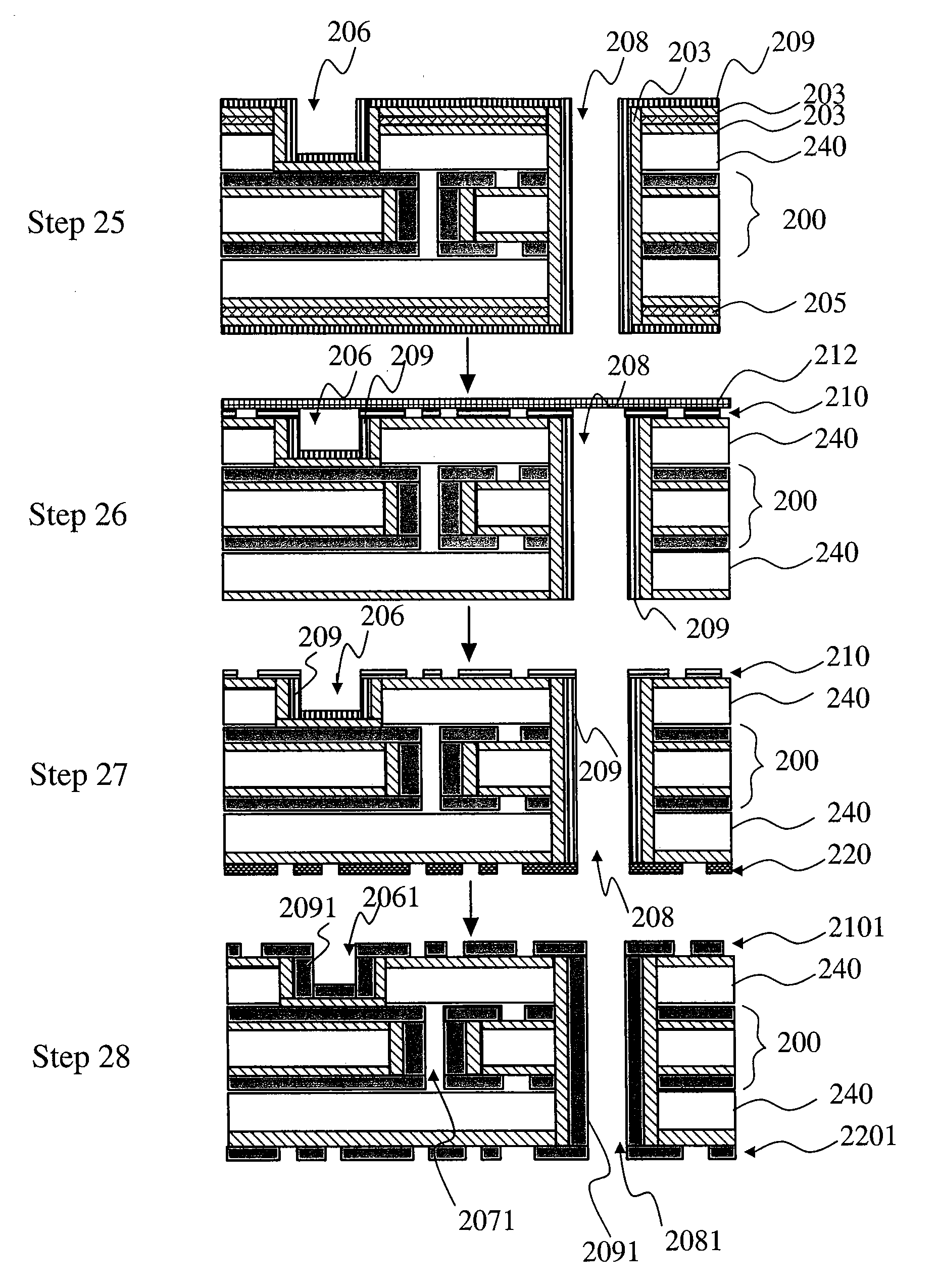
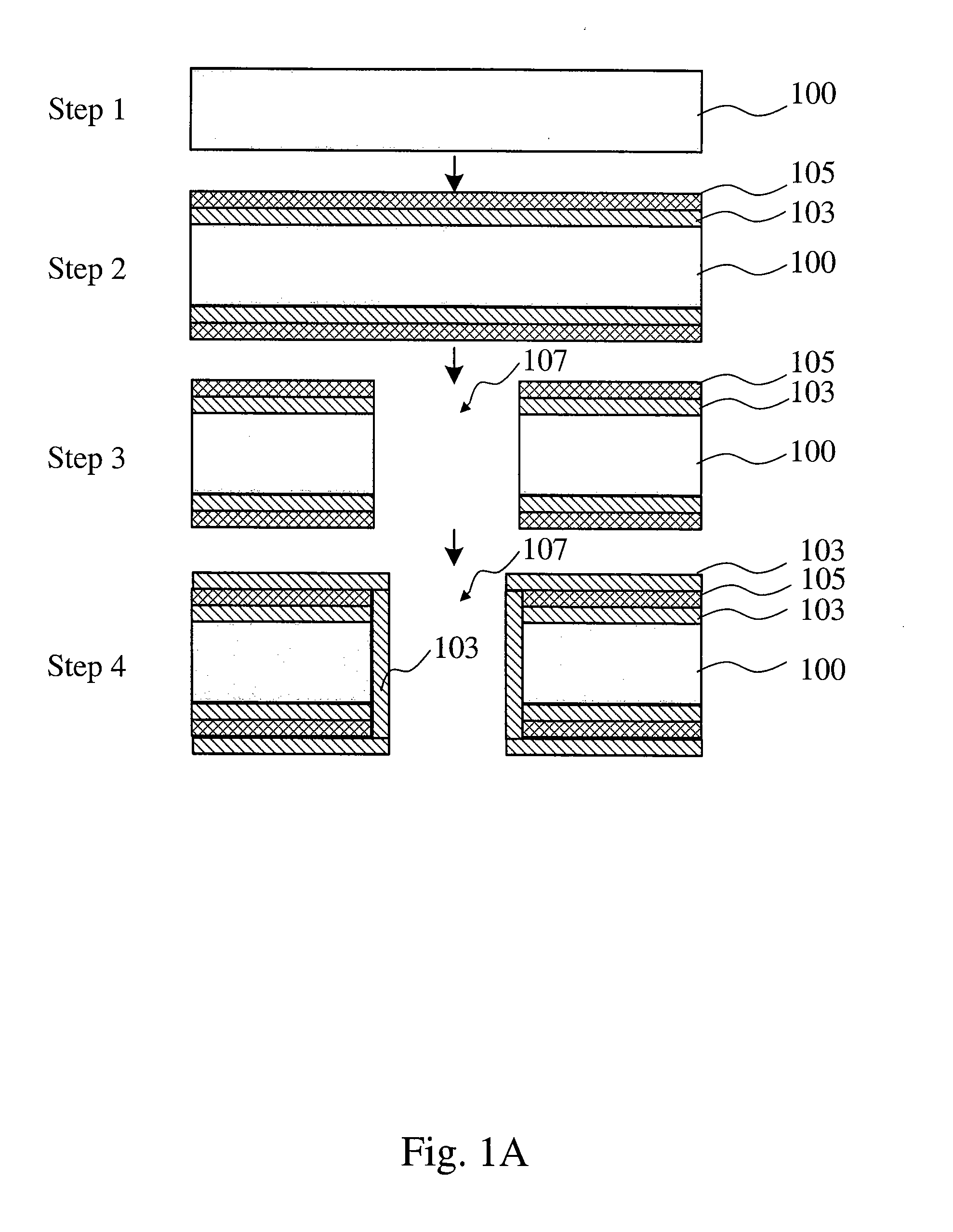
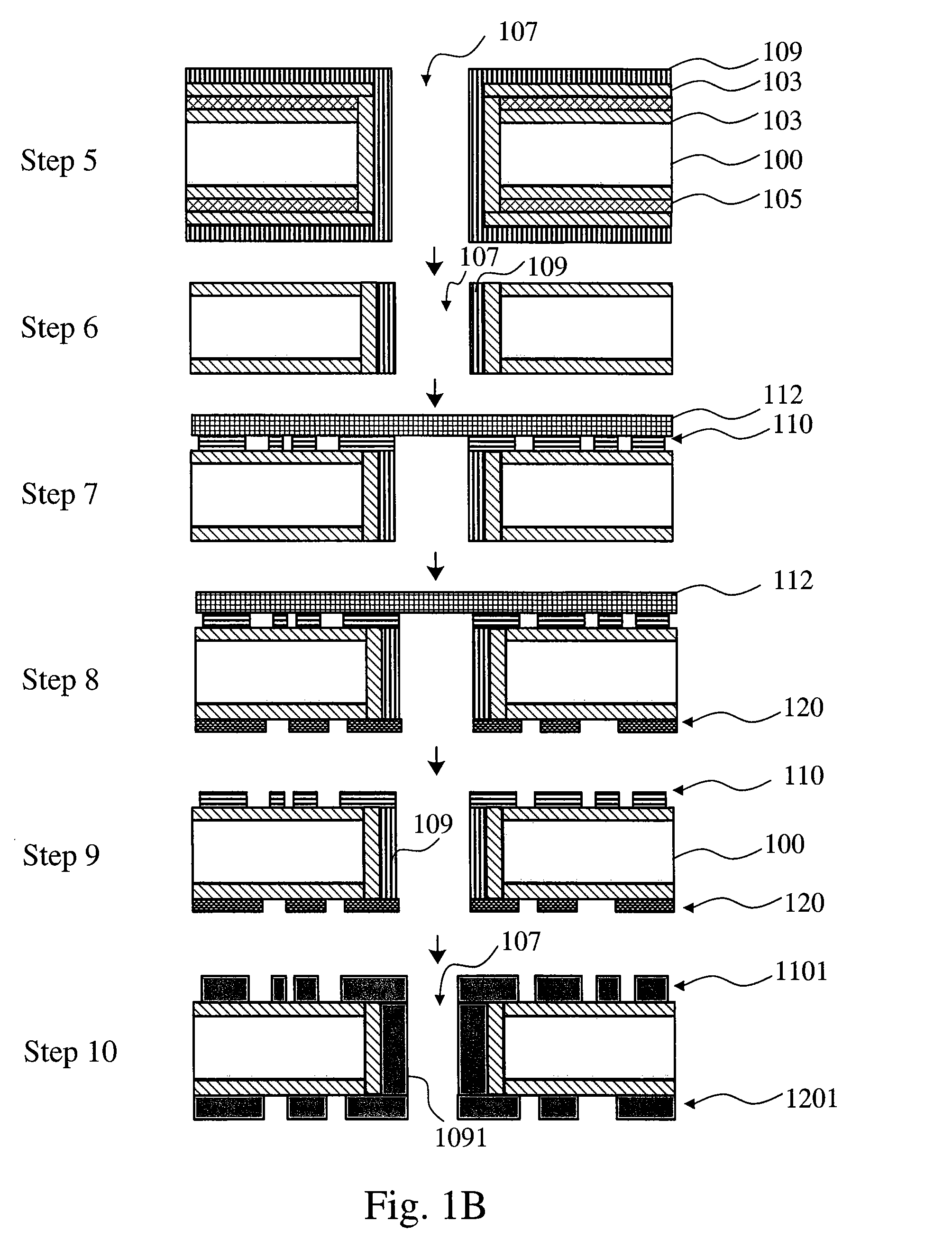
[0004]With the rapid development of electronic products having a reduced size, high-density packaging technology must meet these requirements. A printed circuit board (PCB) is a major device for carrying electronic products. Thus, the manufacturing technology tends to make PCBs lightweight, thin, and having fine lines and mini holes and other high-density designs. A conventional process for fabricating a PCB wiring board includes pressing a metal membrane onto a substrate, coating a photoresist layer via spin coating, and then carrying out the steps of masking exposure, developing, etching, drilling and baking, laminating and plating, and the like. The entire manufacturing process requires repeated testing and repairs. Therefore, the co...
PUM
| Property | Measurement | Unit |
|---|---|---|
| Electric charge | aaaaa | aaaaa |
| aaaaa | aaaaa |
Abstract
Description
Claims
Application Information