Method for power-saving multi-pass sensing in non-volatile memory
a multi-pass sensing and non-volatile memory technology, applied in the field of non-volatile semiconductor memory, can solve the problems of less accurate sensing and more power draining from pre-charged storag
- Summary
- Abstract
- Description
- Claims
- Application Information
AI Technical Summary
Benefits of technology
Problems solved by technology
Method used
Image
Examples
Embodiment Construction
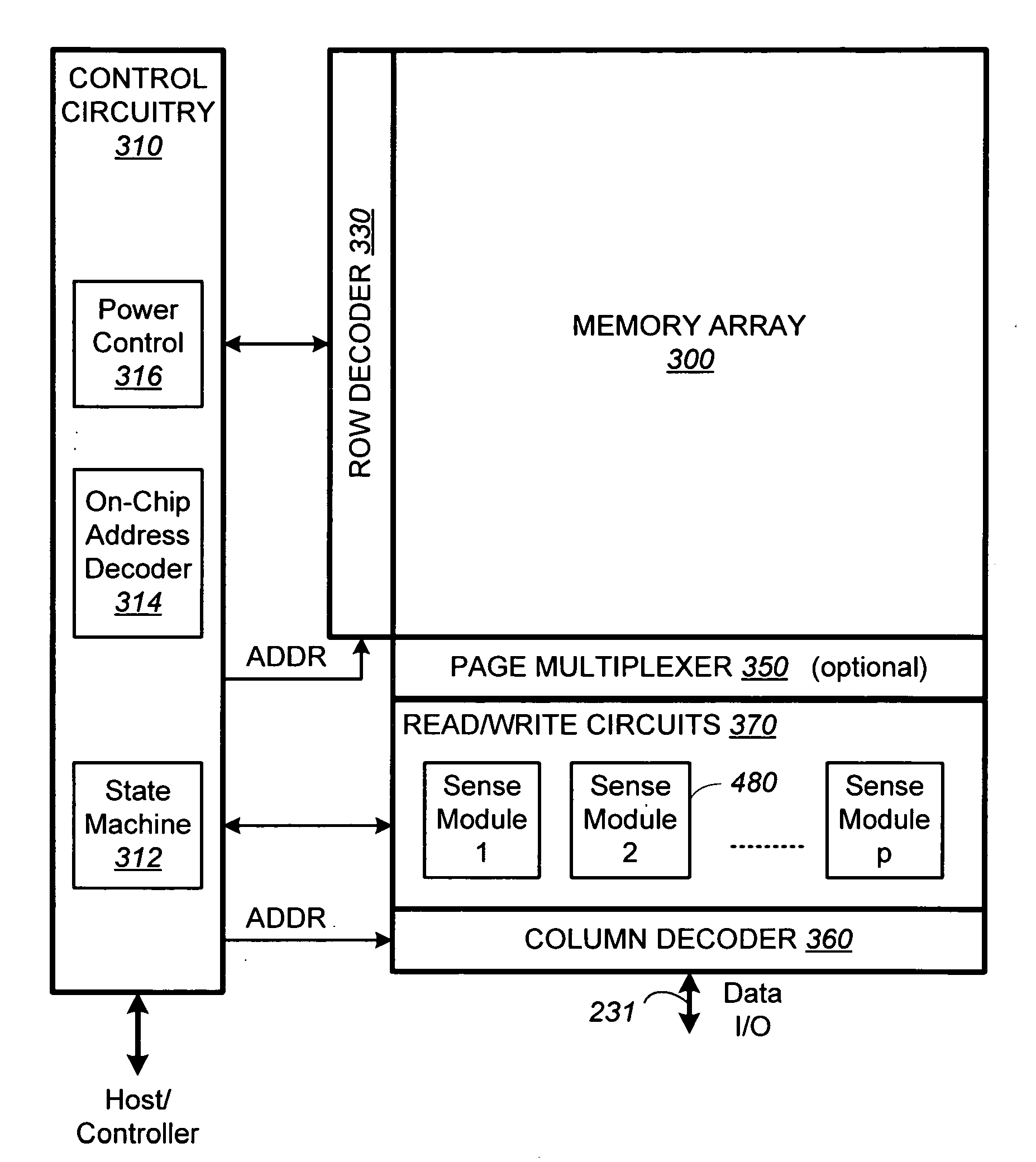
[0075]FIG. 6A illustrates schematically a compact memory device having a bank of read / write circuits, which provides the context in which the present invention is implemented. The memory device includes a two-dimensional array of memory cells 300, control circuitry 310, and read / write circuits 370. The memory array 300 is addressable by word lines via a row decoder 330 and by bit lines via a column decoder 360. The read / write circuits 370 is implemented as a bank of sense modules 480 and allows a block (also referred to as a “page”) of memory cells to be read or programmed in parallel. In a preferred embodiment, a page is constituted from a contiguous row of memory cells. In another embodiment, where a row of memory cells are partitioned into multiple blocks or pages, a block multiplexer 350 is provided to multiplex the read / write circuits 370 to the individual blocks.
[0076] The control circuitry 310 cooperates with the read / write circuits 370 to perform memory operations on the me...
PUM
 Abstract
Description
Claims
Application Information


