Multiple chip module and package stacking method for storage devices

a storage device and chip module technology, applied in the field of computer systems, can solve the problem of limiting the miniaturization of the entire storage device, and achieve the effects of increasing capacity or adding functions, maximizing capacity, and highly reliable module to module relationships

Active Publication Date: 2007-07-12
BITMICRO LLC
View PDF12 Cites 25 Cited by
  • Summary
  • Abstract
  • Description
  • Claims
  • Application Information

AI Technical Summary

Benefits of technology

[0005] In the stacking technique illustrated in example embodiments of the present invention, semiconductor dies are mounted in a module to become a MCM which serves as the basic building block. Combination of these modules and dies in a substrate creates a package with specific function or a range of memory capacity. These packages are stacked to increase capacity or add functions. A combination of different existing technology such as flip chip, wire bond, MCM, module stacking, advance packaging, etc. are used to accomplish highly reliable module to module and package to package interconnection and scalability. A single package can have a wide range of capacity depending on the memory capacity of the die used and the number of modules stacked within the package. In the proposed package stacking technique, the stacked modules in a package serve as the building blocks for the package level stacking. Multiple packages are stacked to create the desired memory capacity and different packages are stacked to create desired function. Expansion can be done both on the vertical and horizontal orientations. The technique is in the assignment of pins. Small capacity miniature storage devices can use the vertical expansion, while high capacity devices with larger form factors can use both vertical and horizontal expansion to maximize capacity. By using this technique, large capacity storage devices are implemented in a small package device, and larger form factors achieve bigger memory capacities.
[0006] The present invention takes advantage of the existing stacking technology both on the module and package level. This maximizes the capacity in a small area, realizing the miniaturization transition. Modular approach is used in creating basic building blocks which can be tested individually and replaced easily prior to final packaging, making the technique reliable, and cost effectively. Wide range of capacity can be configured through variation of die capacities and stacking modules and / or packages. Expansions are implemented both vertically and horizontally depending on board area and desired capacity.

Problems solved by technology

This current method limits the miniaturization of the entire storage device.

Method used


Image

  • Multiple chip module and package stacking method for storage devices
  • Multiple chip module and package stacking method for storage devices
  • Multiple chip module and package stacking method for storage devices

Examples


Embodiment Construction

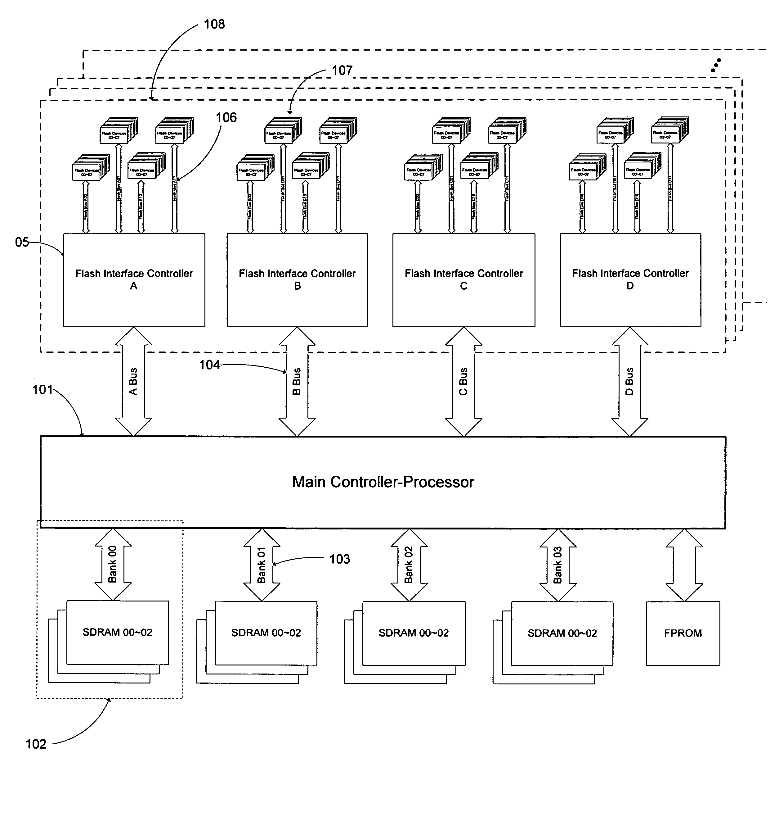
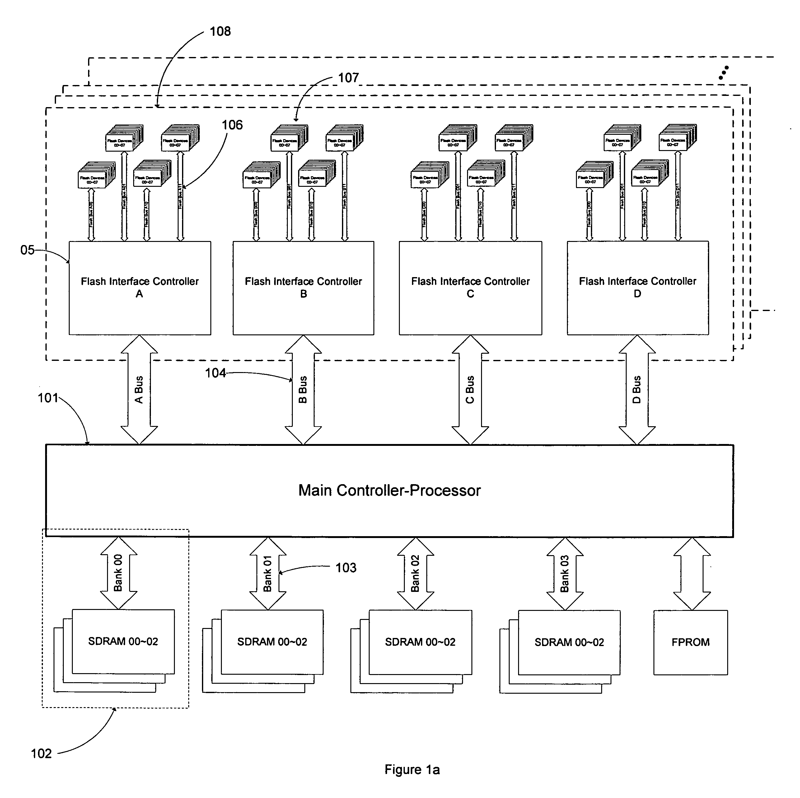
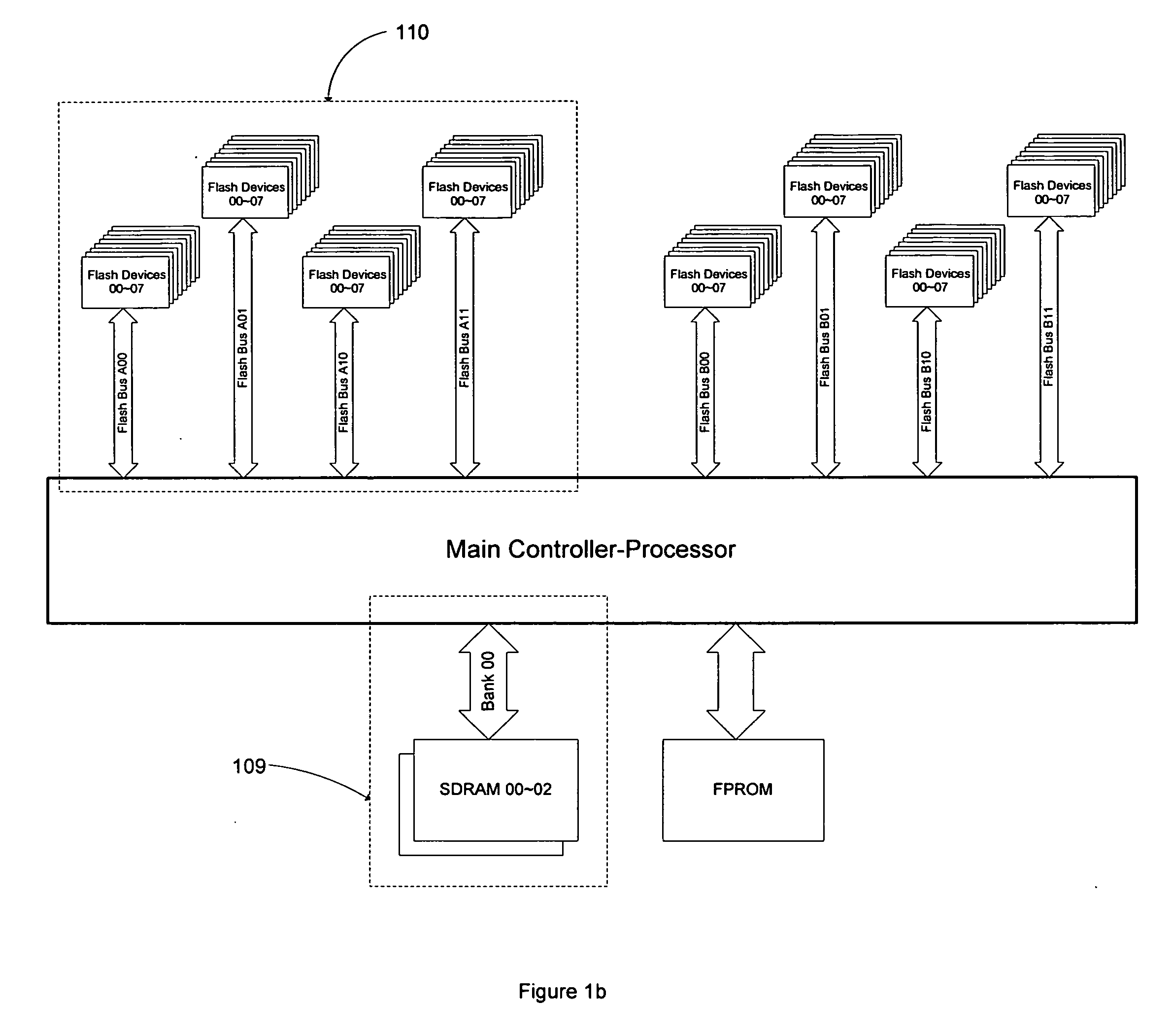
[0034]FIG. 1a is a block diagram of a flash storage system according to a first example embodiment of the present invention. The block diagram shows the entire high-end system that is modularized, stacked, and packaged to achieve the desired features of the technique. The heart of the system is the main controller-processor 101 which interfaces with the flash memory, the flash PROM and the SDRAM memory blocks. The SDRAM is configured from a single bank 102 to a maximum of four banks depending on the desired capacity. Each bank such as 102 includes 3 SDRAMs. The flash devices such as 107 are controlled by the Flash Interface Controller such as 105. Each controller supports four flash buses such as flash bus A11106, and each flash bus supports a maximum of 8 flash devices. The main controller-processor supports four flash interface controllers through 4 different busses such as B bus 104. The four flash interface controllers with their corresponding flash devices comprise the memory s...


PUM


Abstract

Stacking techniques are illustrated in example embodiments of the present invention wherein semiconductor dies are mounted in a module to become a MCM which serves as the basic building block. Combination of these modules and dies in a substrate creates a package with specific function or a range of memory capacity. Several example system configurations are provided using BGA and PGA to illustrate the stacking technique. Several pin assignment and signal routing techniques are illustrated wherein internal and external signals are routed from main board to various stacked modules. Expansion can be done both on the vertical and horizontal orientations.

Description

BACKGROUND [0001] 1. Field [0002] The present invention relates to computer systems. More particularly, the present invention relates to flash memory based semiconductor disk drive and a method of using multiple chip module (MCM) and Package Stacking technique to support miniaturization and memory scalability. [0003] 2. Description of Related Art [0004] Flash memory based semiconductor disk drive typically use separate packages for the interface controller, the DMA controller, the processor and separate packages for the Flash devices, the FPROMs and the RAMs. This current method limits the miniaturization of the entire storage device. In order to achieve the move to miniaturization, chip modules and packages need to be stacked. Stacking both on chip module and package level maximizes the capacity in a limited area thus realizing the move to miniaturize the entire storage device. A technique in stacking chip modules and packages strategically to support miniaturization and memory sca...

Claims


Application Information

Patent Timeline
Patent Type & Authority Applications(United States)
IPC IPC(8): H01L23/02
CPCH01L24/16H01L25/0655H01L25/105H01L25/18H01L2225/1005H01L2924/01079H01L2924/15331H01L2225/1023H01L2225/1058H01L2224/16H01L2924/1627H01L23/02H01L23/12
Inventor BRUCE, REYBRUCE, RICARDOBUGAYONG, PATRICK DIGAMONBAYLON, JOEL ALONZO
Owner BITMICRO LLC
Why Eureka
Try Eureka