HEMT piezoelectric structures with zero alloy disorder

a piezoelectric structure and alloy disorder technology, applied in the field of manufacturing semiconductor substrates, can solve the problems of non-homogeneous distribution of ga and al atoms in the barrier layer, the reliability of transistor structures made on the semiconductor material, and the reliability of the structure of the semiconductor material. achieve the effect of high-quality piezoelectric properties

Inactive Publication Date: 2007-07-19
PICOGIGA INT
View PDF17 Cites 20 Cited by
  • Summary
  • Abstract
  • Description
  • Claims
  • Application Information

AI Technical Summary

Benefits of technology

[0033] The present invention relates to a piezoelectric structure comprising a semi-conducting substrate based on elements in Groups III and V of the periodic table, with the Group V element preferably being nitrogen. The substrate typically includes a support, a channel layer on the support and a ba...

Problems solved by technology

These parameters are related to methods of producing the semiconductor structure based on Type III-Type N, and generate problems with the reliability of transistor structures made on the semiconductor material.
A drawback of the semi-conducting material of the prior art is the non-homogeneous distribution of Ga and Al atoms in the barrier layer 40.
The process disclosed in WO02/093650 allows increasing the electron mobility within the structure, but it does not address the issue of increasing the homogeneity of the electron distribution (particularly in the channel layer).
And in this respect the process disclosed by WO02/09365...

Method used


Image

  • HEMT piezoelectric structures with zero alloy disorder
  • HEMT piezoelectric structures with zero alloy disorder
  • HEMT piezoelectric structures with zero alloy disorder

Examples


first embodiment

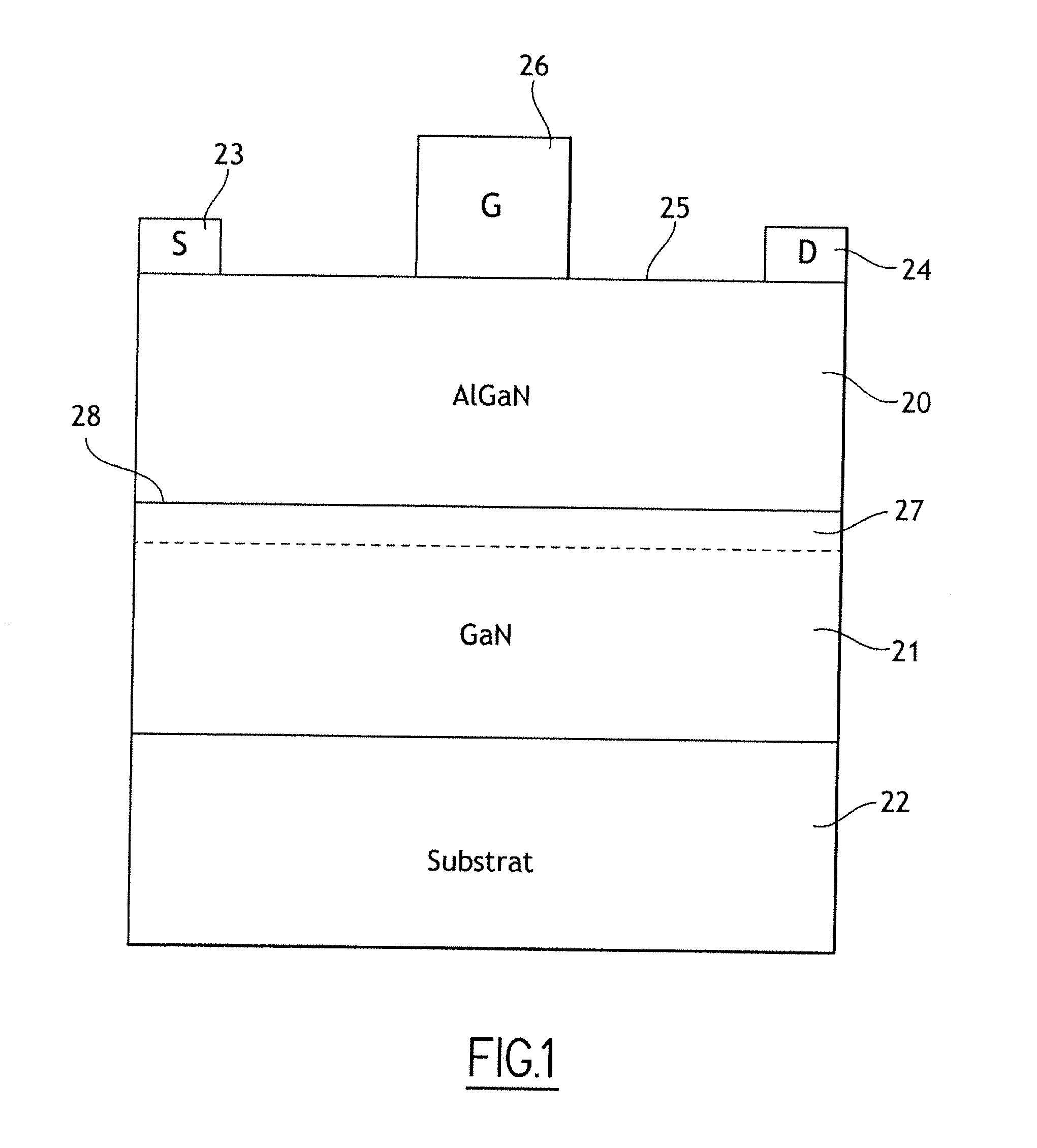
[0089]FIG. 7a illustrates a semiconductor structure 50 according to the invention. This semiconductor structure 50 comprises a channel layer 51 on a support 52, and a barrier layer 53 made of a ternary pseudo-alloy on the channel layer 51. The support 52 is made of SiC. However, the support could be made of other materials such as Silicon, AlN, sapphire or GaN. The channel layer 51 is a binary alloy of GaN. However, another material could have been chosen for the channel layer 51, such as AlN, BN (boron nitride) or InN (indium nitride). The channel layer 51 is deposited on the support by a method known to those skilled in the art such as Molecular Beam Epitaxy (MBE) or Metal-Organic Chemical Vapor Deposition (MOVD) method.

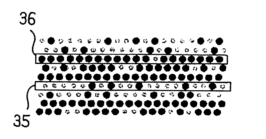
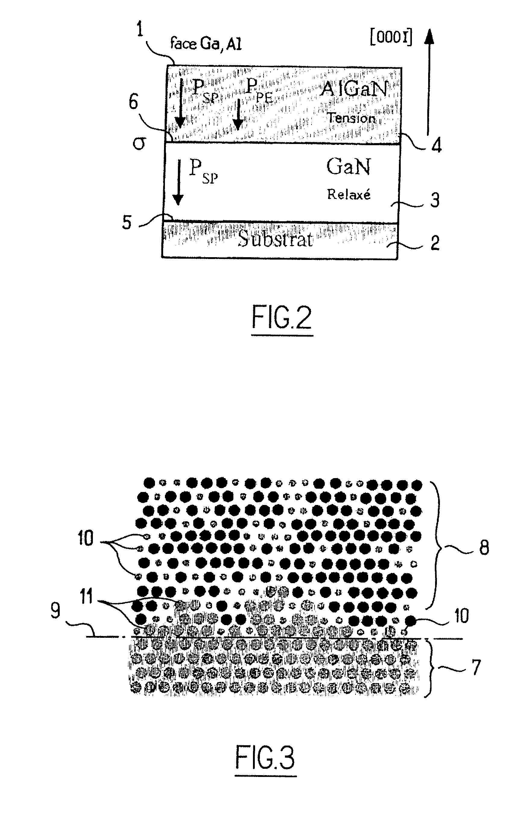
[0090] The barrier layer 53 is a ternary pseudo-alloy of AlGaN. The barrier layer 53 comprises binary alloy layers of GaN 54 and binary alloy layers of AlN 55. The GaN and AlN layers are supplied in an alternating fashion. Each binary alloy layer made of GaN 54 (or...

fourth embodiment

[0117]FIG. 7d illustrates a semiconducting material according to a This semiconducting material includes a support 52, a buffer layer 56, a channel layer 51 and a barrier layer 53. In this embodiment, the buffer layer 56 is a ternary pseudo-alloy of AlGaN composed of alternating layers of binary alloy of GaN 57 and binary alloy of AlN 58. The buffer layer 56 has the same characteristics as the ternary pseudo-alloy barrier layer (nGaN and nAlN between 1 and 40, preferably between 1 and 20, and even more preferably between 2 and 10 and possibly varying along the buffer layer, etc.).

[0118] In this embodiment, the buffer layer 56 comprises two GaN layers 57 alternating with two AlN layers 58. Furthermore, the number of atomic monolayers nGaN per GaN layer 57 varies along the buffer layer 56. The GaN layer 57 closest to the support comprises two atomic monolayers while the GaN layer furthest from the support comprises four atomic monolayers. The number of atomic monolayers nAlN per AlN ...


PUM


Abstract

Electronic circuits dedicated to high frequency and high power applications based on gallium nitride (GaN) suffer from reliability problems. The main reason is a non-homogenous distribution of the electronic density in these structures that originates from alloy disorders at the atomic and micrometric scale. This invention provides processes for manufacturing semiconducting structures based on nitrides of Group III elements (Bal, Ga, In)/N which are perfectly ordered along a preferred crystalline axis. To obtain this arrangement, the ternary alloy barrier layer is replaced by a barrier layer composed of alternations of binary alloy barrier layers. The lack of fluctuation in the composition of these structures improves electron transport properties and makes the distribution more uniform.

Description

CROSS-REFERENCE TO RELATED APPLICATIONS [0001] This application is a continuation of International Application PCT / EP2005 / 054559 filed Sep. 13, 2005. This application is also continuation-in-part of U.S. application Ser. No. 11 / 004,411 filed Dec. 3, 2004. The entire content of each application is expressly incorporated herein by reference thereto.FIELD OF THE INVENTION [0002] This invention generally relates to manufacturing semiconductor substrates for use in making electronic components. The technical domain of the invention may be defined in general as preparation of layers of semiconducting materials based on nitride on a support. In particular, the invention pertains to a piezoelectric semiconductor structure that includes a support substrate, a channel layer arranged on one side of the support substrate, and a barrier layer formed on the channel layer. The barrier layer preferably comprises alternating binary alloy layers of Type III-Type V semiconductor materials. BACKGROUND ...

Claims


Application Information

Patent Timeline
IPC IPC(8): H01L33/00
CPCH01L29/155H01L29/7787H01L29/2003H01L29/778H01L29/20
Inventor LAHRECHE, HACENEBOVE, PHILIPPE
Owner PICOGIGA INT
Why Eureka
Try Eureka