Inorganic electroluminescent diode and method of fabricating the same

Active Publication Date: 2007-07-26
SAMSUNG ELECTRONICS CO LTD
View PDF10 Cites 52 Cited by
  • Summary
  • Abstract
  • Description
  • Claims
  • Application Information

AI Technical Summary

Benefits of technology

[0010]In another embodiment, an inorganic electroluminescent diode composed completely of ino

Problems solved by technology

In the electroluminescent diode of the above patent, organic/inorganic interfacial defects may occur because the organic thin film layers are in contact with the inorganic luminescent layer, and thus, stability is decreased upon operation of the device.
As a

Method used


Image

  • Inorganic electroluminescent diode and method of fabricating the same
  • Inorganic electroluminescent diode and method of fabricating the same
  • Inorganic electroluminescent diode and method of fabricating the same

Examples


Example

EXAMPLE 1

Fabrication of Electroluminescent Diode of Crystalline HTL and Amorphous ETL Structure

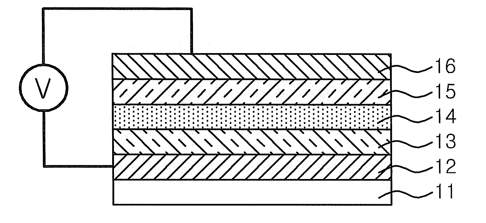
[0052]In FIG. 3, on one surface of a sapphire substrate 31, palladium was deposited to a thickness of 50 nm by thermal evaporation, followed by deposition of gold (Au) to a thickness of 200 nm was deposited, thus forming a palladium / gold alloyed electrode 32. Thereafter, a p-doped crystalline GaN thin film having a thickness of 2.5 μm was grown on the sapphire substrate 31 by MOCVD. Further, a hole transport layer (“HTL”) 33 was grown to a thickness of 200 nm at a substrate temperature of 1050° C.

[0053]On the GaN thin film, a solution of 0.3 wt % of red CdSe / ZnS core / shell nanocrystals (Evidot® 630 nm absorbance) (Evident Technology, trade name: Evidot® Red (CdSe / ZnS)) in chloroform was dispensed and spin coated at 2000 rpm for 30 sec, and then dried at 50° C. for 5 min, thus forming a semiconductor nanocrystal layer 34 of 25 nm thickness.

[0054]Subsequently, TiO2 was applied to a thickness...

Example

EXAMPLE 2

Fabrication of Electroluminescent Diode of Crystalline HTL and Liquid Amorphous ETL Structure

[0056]On a sapphire substrate, a p-doped crystalline GaN thin film was grown to a thickness of 200 nm at a substrate temperature of 1050° C. by MOCVD, thus forming a hole transport layer. On the p-doped crystalline GaN thin film, a solution of 0.3 wt % of red CdSe / ZnS core / shell nanocrystals in chloroform was dispensed and spin coated at 2000 rpm for 30 sec, and then dried at 50° C. for 5 min, thus forming a semiconductor nanocrystal layer of 25 nm thickness.

[0057]Thereafter, an SiO2 thin film about 1 nm thick was formed on the completely dried semiconductor nanocrystal layer by e-beam evaporation, thus forming a protective layer. Then, TiO2 precursor sol (DuPont Tyzor® BTP, 2.5 wt % in butanol) was spin coated at 2000 rpm for 30 sec on the protective layer, dried for about 5 min at 50° C., and annealed at 100° C. for 30 min, thus forming an electron transport layer in the form of a...

Example

EXAMPLE 3

Fabrication of Quantum Dot Electroluminescent Diode of Amorphous (CdTe, HTL) and Amorphous (TiO2, ETL) Structure

[0059]A glass substrate having ITO features patterned thereon was sequentially washed with neutral detergent, deionized water, water, and isopropyl alcohol, and then was subjected to UV-ozone treatment, and a CdTe thin film of 40 nm thickness was subsequently vacuum deposited on the ITO substrate. The temperature of the substrate was maintained at about 200° C., and an amorphous CdTe thin film about 40 nm thickness was formed. Subsequently, a semiconductor nanocrystal layer, an ETL, and an electrode were sequentially deposited on the CdTe thin film in the same manner and having the same thicknesses as provided in Example 1, thus fabricating an inorganic electroluminescent diode.

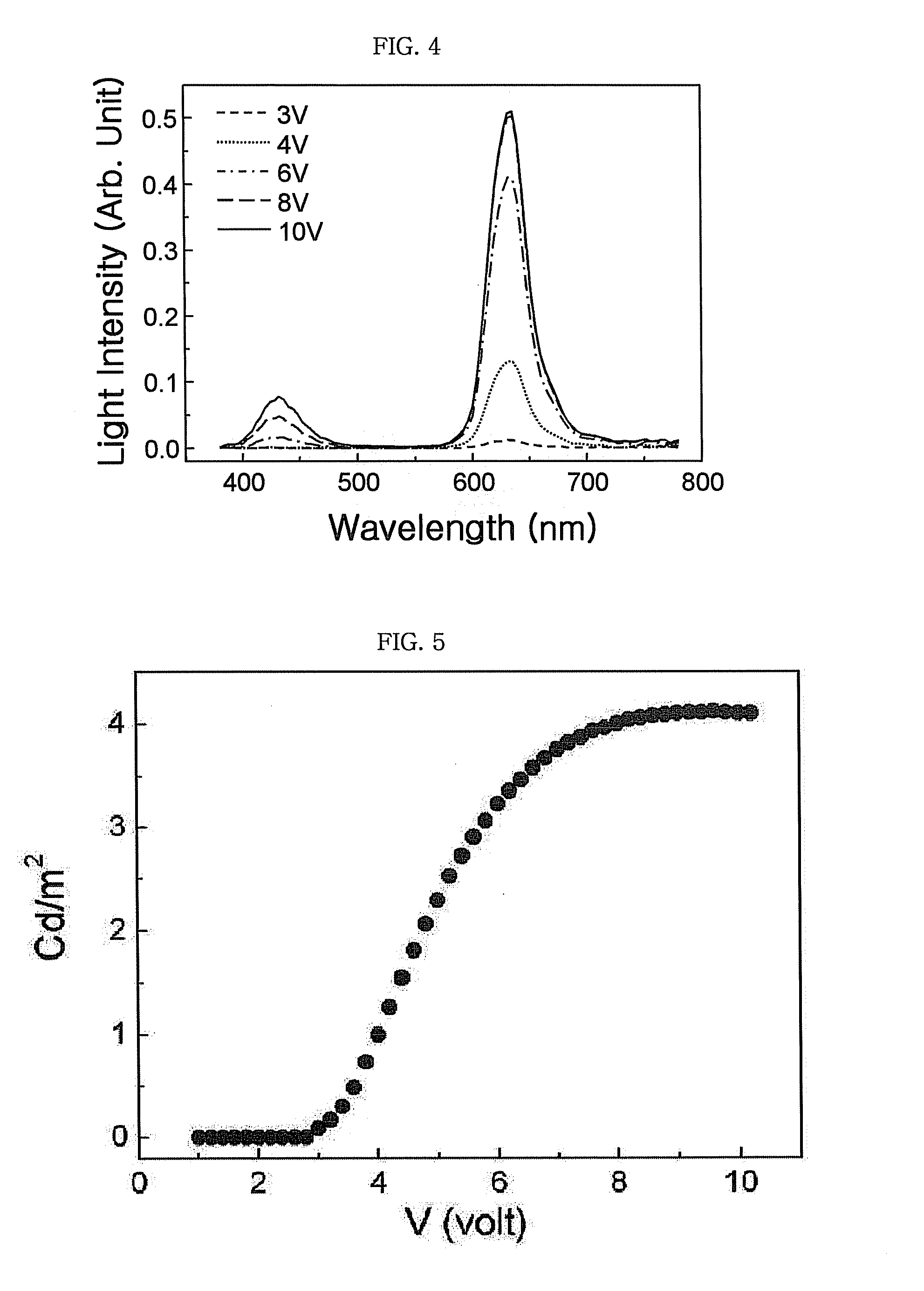
[0060]FIG. 4 shows the light intensity of the inorganic electroluminescent diode fabricated in Example 1. As shown in FIG. 4, the above electroluminescent diode was confirmed to emit light ...


PUM


Abstract

Disclosed are an inorganic electroluminescent diode and a method of fabricating the same. Specifically, this invention provides an inorganic electroluminescent diode, which includes a semiconductor nanocrystal layer formed of inorganic material, an electron transport layer or a hole transport layer formed on the semiconductor nanocrystal layer using amorphous inorganic material, and a hole transport layer or an electron transport layer formed beneath the semiconductor nanocrystal layer using inorganic material, and also provides a method of fabricating such an inorganic electroluminescent diode. According to the method of fabricating the inorganic electroluminescent diode of this invention, an inorganic electroluminescent diode can be fabricated while maintaining the properties of luminescent semiconductor material of the semiconductor crystal layer, and also an inorganic electroluminescent diode which is stably operated and has high luminescent efficiency can be provided.

Description

[0001]This application claims priority to Korean Patent Application No. 2006-2189, filed on Jan. 9, 2006, and all the benefits accruing therefrom under U.S.C. § 119(a) which is incorporated herein in its entirety by reference.BACKGROUND OF THE INVENTION[0002]1. Field of the Invention[0003]The present invention relates, generally, to an inorganic electroluminescent diode and a method of fabricating the same, and more particularly, to an inorganic electroluminescent diode, comprising a semiconductor nanocrystal layer formed of inorganic material, an electron transport layer or a hole transport layer formed on the semiconductor nanocrystal layer using amorphous inorganic material, and a hole transport layer or an electron transport layer formed beneath the semiconductor nanocrystal layer using inorganic material, and to a method of fabricating such an inorganic electroluminescent diode.[0004]2. Description of the Related Art[0005]Various attempts have been made to solve a problem of a ...

Claims


Application Information

Patent Timeline
IPC IPC(8): H01L33/00H01L33/06H01L33/08H01L33/18H01L33/26
CPCC09K11/565C09K11/883H01L33/06H05B33/14H01L33/18H01L33/26H01L33/08E03F5/021
Inventor CHO, KYUNG SANGKIM, BYUNG KICHOI, BYOUNG LYONGKWON, SOON JAE
Owner SAMSUNG ELECTRONICS CO LTD
Why Eureka
Try Eureka