Excimer laser and line narrowing module

a laser and laser technology, applied in the field of semiconductor manufacturing equipment, can solve the problems of low production yield and achieve the effect of maximizing production yield

Inactive Publication Date: 2007-07-26
SAMSUNG ELECTRONICS CO LTD
View PDF7 Cites 3 Cited by
  • Summary
  • Abstract
  • Description
  • Claims
  • Application Information

AI Technical Summary

Benefits of technology

[0015]Therefore, the present invention provides an excimer laser and LNM in which the DOF and margin of excimer laser light focused on a layer of photoresist of a wafer via a reduction-projection lens of an exposure apparatus is increased to avoid exposure failure, thereby increasing and maximizing production yields.

Problems solved by technology

When the DOF is lowered, exposure failure may occur leading to lower production yields.

Method used


Image

  • Excimer laser and line narrowing module
  • Excimer laser and line narrowing module
  • Excimer laser and line narrowing module

Examples


Embodiment Construction

[0026]The present invention will now be described with reference to the accompanying drawings in which exemplary embodiments of the invention are illustrated. This invention, however, may be embodied in many different forms and should not be construed as being limited to the embodiments set forth herein. Rather, these embodiments are provided so that this disclosure will be thorough and complete, and will fully convey the scope of the invention to those skilled in the art.

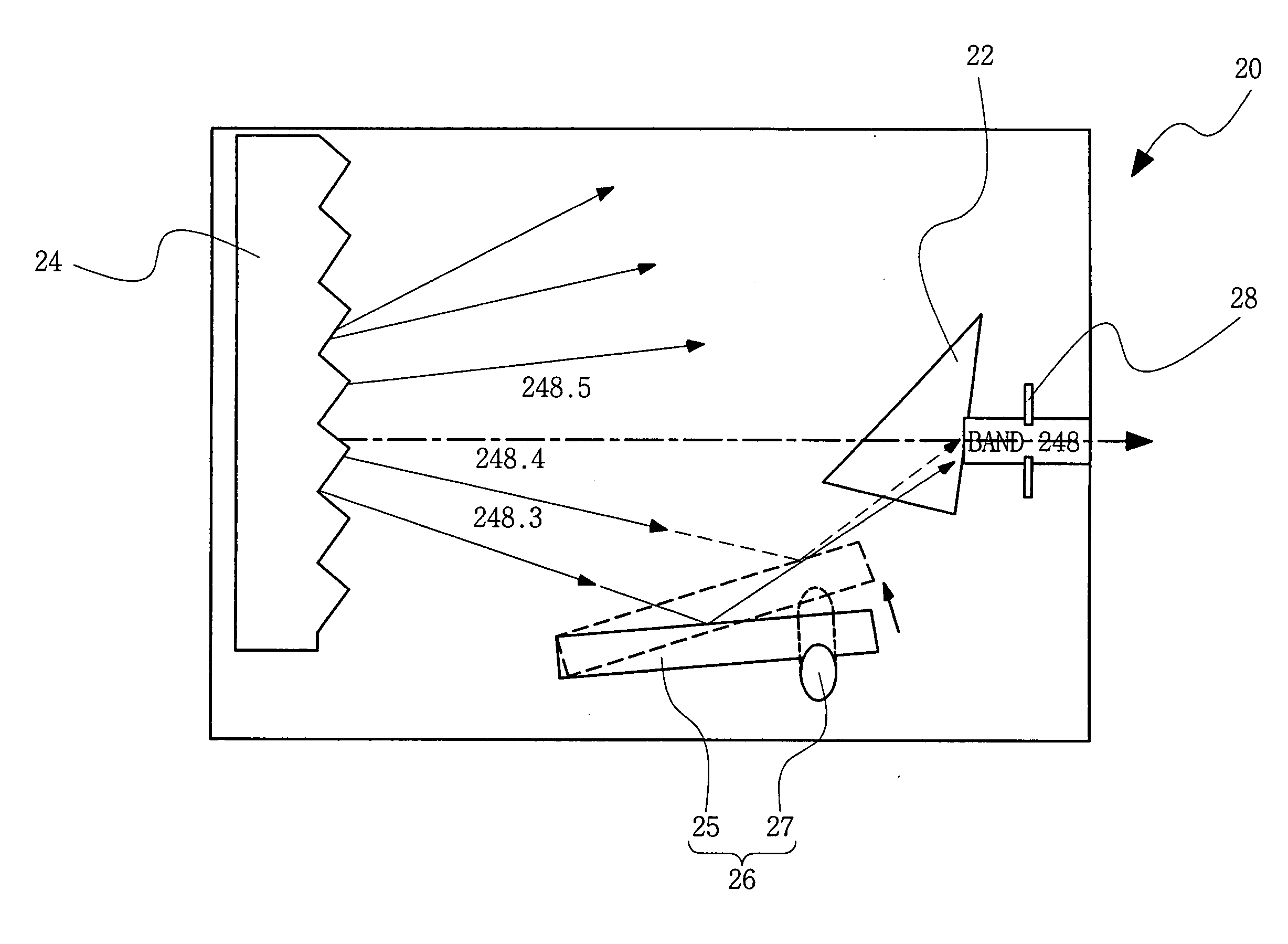
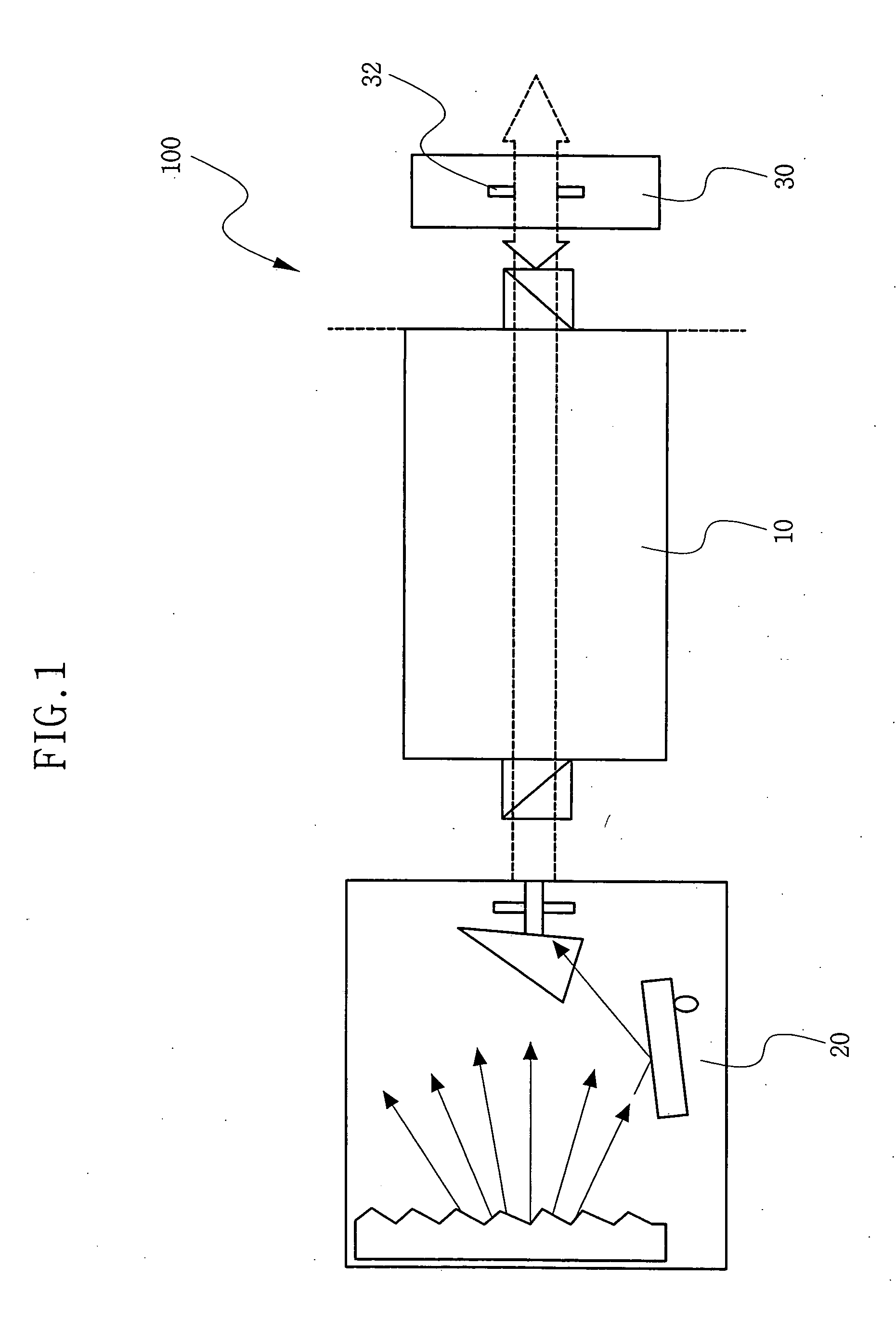
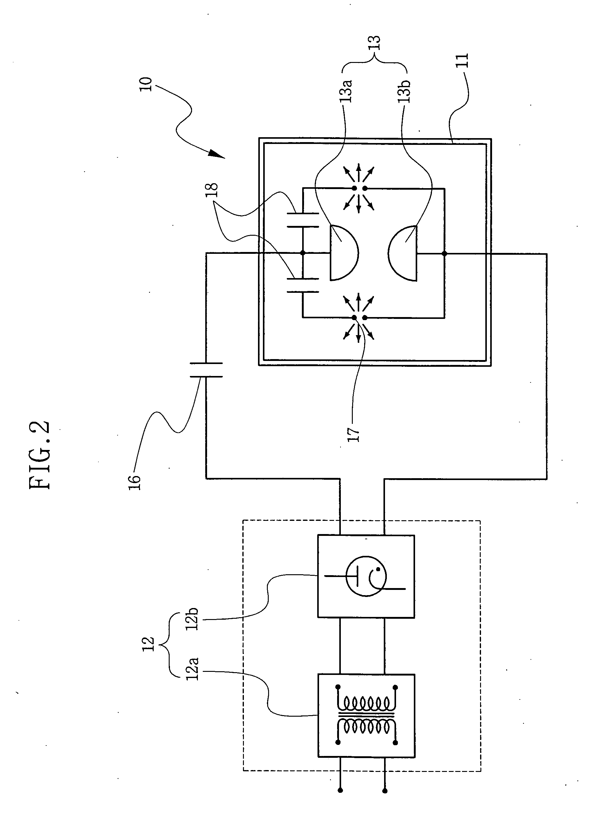
[0027]FIG. 1 is a diagram illustrating an excimer laser 100 according to an exemplary embodiment of the present invention. An excimer laser 100 is composed of a generator 10, a line narrowing module 20, and an output coupler 30. Generator 10 is used for exciting a light emitting material such as a halogen or inert gas to produce excimer laser light. The line-narrowing module (LNM) 20 communicates with generator 10 and is used to line-narrow the excimer laser light produced by generator 10 and feeds back the laser l...


PUM


Abstract

An excimer laser and a line-narrowing module capable of increasing and maximizing production yield in semiconductor manufacturing are disclosed. The line-narrowing module utilizes a beam expander that passes laser light, produced by and incident from a generator of the excimer laser and collimates the laser light in one direction. A diffraction grating receives the collimated laser light and diffracts the laser light and causes a traveling direction of the laser light to be separated according to an associated wavelength of the laser light. A multi-wavelength reflector located at a reflecting position on one side between the diffraction grating and the beam expander in order to re-enter the laser light having a multi-wavelength into the generator through the beam expander. The multi-wavelength reflector reflects the laser light consisting of a plurality of wavelengths among the laser light whose traveling direction is separated from the diffraction grating onto the beam expander.

Description

BACKGROUND OF THE INVENTION[0001]1. Technical Field[0002]Embodiments of the invention relate to semiconductor manufacturing equipment, and more particularly, to an excimer laser used as a light source in an exposure apparatus for photosensitizing photoresist formed on a wafer, and a line narrowing module associated therewith.[0003]This application claims the benefit of Korean Patent Application No. 10-2006-0006081, filed Jan. 20, 2006, the disclosure of which is hereby incorporated herein by reference in its entirety.[0004]2. Discussion of Related Art[0005]Currently, with the rapid development of the information telecommunication field and the popularization of information media such as computers, semiconductor equipment is being remarkably developed. The use of semiconductors is required to ensure high-speed operation of these devices, as well as providing mass storage capacity. Thus, technology of fabricating semiconductor devices is developed to maximize integration density, reli...

Claims


Application Information

Patent Timeline
Patent Type & Authority Applications(United States)
IPC IPC(8): H01S3/22H01S3/08
CPCG03F7/70025G03F7/70575H01S3/036H01S3/2256H01S3/0812H01S3/105H01S3/225H01S3/041
Inventor KIM, JANG-SUN
Owner SAMSUNG ELECTRONICS CO LTD
Why Eureka
Try Eureka