Method of forming self-aligned contact via for magnetic random access memory

a random access memory and contact via technology, applied in the manufacture/treatment of galvano-magnetic devices, basic electric elements, electric devices, etc., can solve the problems of high frequency shorting or opening of devices, difficult memory fabrication, and increased difficulty in forming devices. achieve the effect of increasing the level of device integration

Inactive Publication Date: 2007-07-26
IND TECH RES INST
View PDF4 Cites 19 Cited by
  • Summary
  • Abstract
  • Description
  • Claims
  • Application Information

AI Technical Summary

Benefits of technology

[0010] Accordingly, at least one objective of the present invention is to provide a method of forming a self-aligned contact via for a magnetic random access m

Problems solved by technology

The connection between the magnetic memory cell and the bit line is vulnerable to minor offset in the photolithographic and etching process so that a shorting or an opening of the device occurs with higher frequency.
In other words, the device is more

Method used


Image

  • Method of forming self-aligned contact via for magnetic random access memory
  • Method of forming self-aligned contact via for magnetic random access memory
  • Method of forming self-aligned contact via for magnetic random access memory

Examples


Embodiment Construction

[0024] Reference will now be made in detail to the present preferred embodiments of the invention, examples of which are illustrated in the accompanying drawings. Wherever possible, the same reference numbers are used in the drawings and the description to refer to the same or like parts.

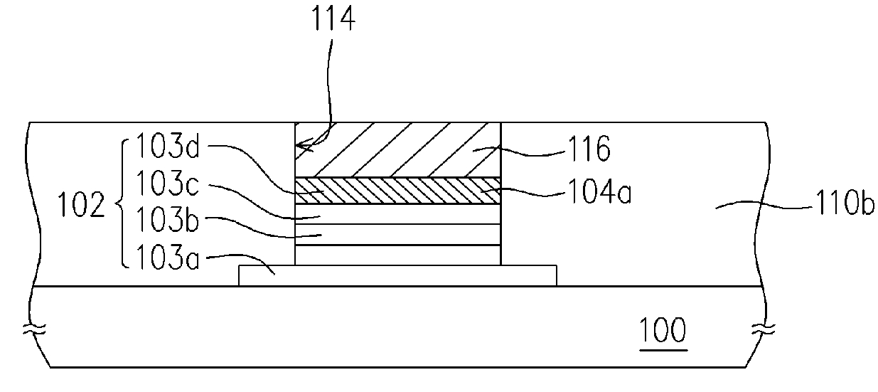
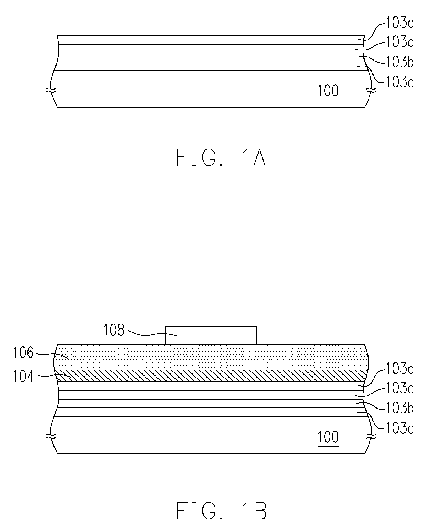
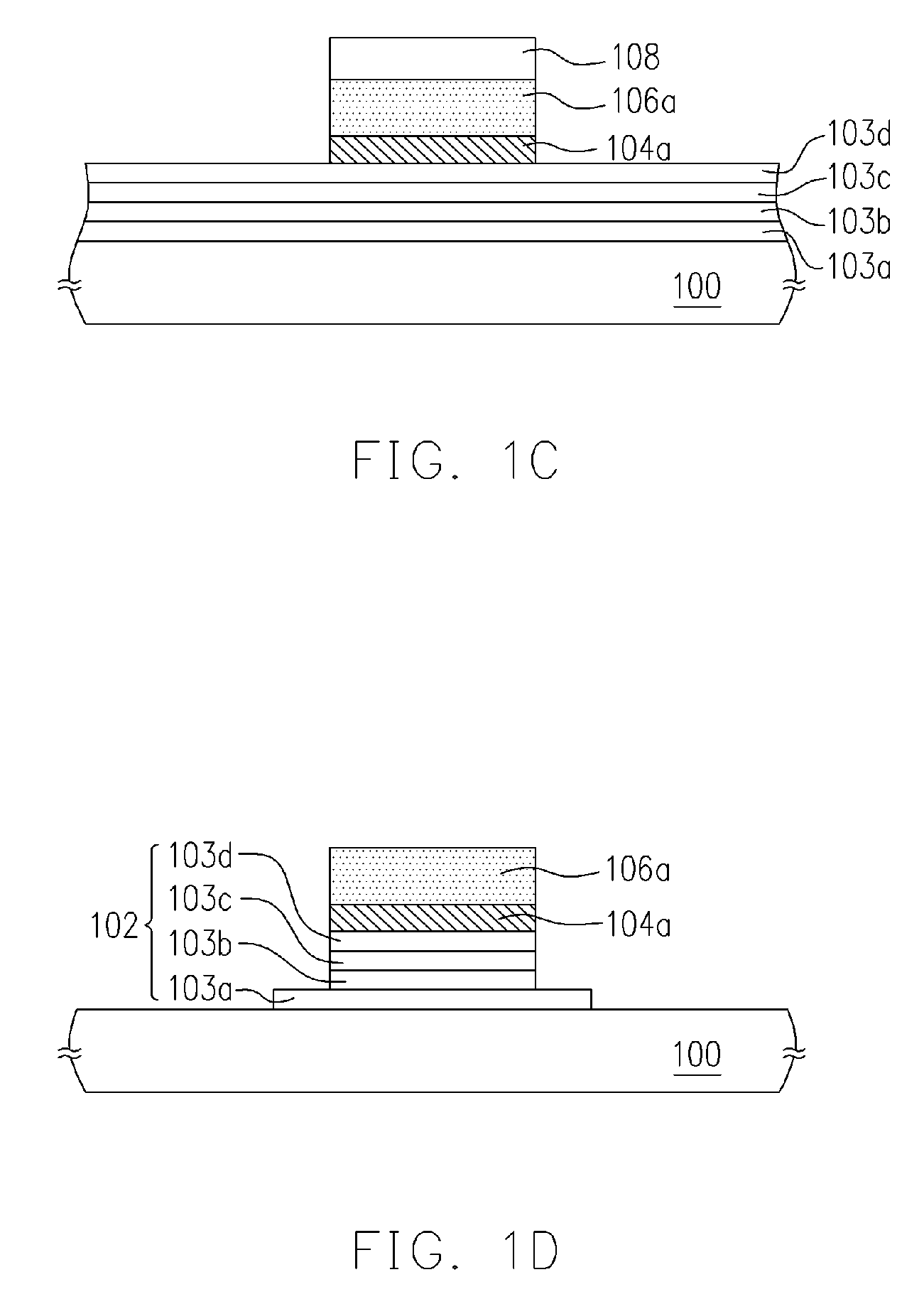
[0025]FIGS. 1A through 1H are schematic cross-sectional views showing the process of forming a self-aligned contact via for a magnetic random access memory according to one embodiment of the present invention. As shown in FIG. 1A, a substrate 100 is provided. The substrate 100 has a plurality of transistors and metallic interconnects (not shown) already formed therein. Then, a conductive layer 103a, a pinned layer 103b, a tunneling barrier layer 103c and a free layer 103d are sequentially formed over the substrate 100. The conductive layer 103a serves as a bottom electrode of the magnetic random access memory (MRAM) device. The conductive layer 103a comprises tantalum (Ta), tantalum nitride (TaN), ...


PUM


Abstract

A method of forming a self-aligned contact via for a MRAM is disclosed. A first conductive layer, a pinned layer, a tunneling barrier layer, a free layer, a capping layer and a first dielectric layer are formed sequentially over a substrate has formed lots of transistors and interconects. A portion of the first dielectric layer and the capping layer are removed until a surface of the free layer is exposed. A portion of the pinned layer, the tunneling barrier layer and the free layer are removed to form a MRAM device. A second dielectric layer is formed over the magnetic random access memory device. A planarization process is performed to form a planar surface of the second dielectric layer. The first dielectric layer and a portion of the second dielectric layer are removed to form a self-aligned contact opening. A second conductive layer is filled into the self-aligned contact opening.

Description

CROSS-REFERENCE TO RELATED APPLICATION [0001] This application claims the priority benefit of Taiwan application serial no. 95101043, filed on Jan. 11, 2006. All disclosure of the Taiwan application is incorporated herein by reference. BACKGROUND OF THE INVENTION [0002] 1. Field of the Invention [0003] The present invention relates to a method of forming a contact via. More particularly, the present invention relates to a method of forming a self-aligned contact via for a magnetic random access memory (MRAM). [0004] 2. Description of the Related Art [0005] Magnetic random access memory (MRAM) is a non-volatile, high-density, fast read / write and radiation-resistant memory device. MRAM is widely used in portable electronic products and advanced mobile digital and network communication instruments. To write data into the MRAM, the most common method includes choosing two current lines such as a bit line and a write word line and alternatively selecting the magnetic memory cell to be wr...

Claims


Application Information

Patent Timeline
IPC IPC(8): H01L21/00
CPCH01L43/12H10N50/01
Inventor YEN, CHENG-TYNGCHEN, WEI-CHUANSHEN, KUEI-HUNG
Owner IND TECH RES INST
Why Eureka
Try Eureka