Method for fabricating a PCB

Inactive Publication Date: 2007-08-02
FREESCALE SEMICON INC
View PDF11 Cites 7 Cited by
  • Summary
  • Abstract
  • Description
  • Claims
  • Application Information

AI Technical Summary

Problems solved by technology

Some of the problems with traditional PCB fabrication are inherent in the commonly used processes of drilling, chemical etching, and electroplating.
Currently, it is difficult to form a via that is as small as 75 μm in diameter.
Since engineers are constantly striving to reduce the size of the circuitry in all electronics to improve performance and speed, this is a limiting factor.
In additi

Method used


Image

  • Method for fabricating a PCB
  • Method for fabricating a PCB
  • Method for fabricating a PCB

Examples


Embodiment Construction

[0014] A method and an apparatus for fabricating a PCB are provided. In the following description, numerous specific details are set forth in order to provide a thorough understanding of the present invention. It will be understood, however, to one skilled in the art, that the present invention may be practiced without some or all of these specific details. In other instances, well known process operations have not been described in detail in order not to unnecessarily obscure the present invention.

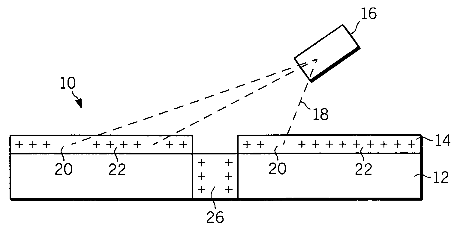
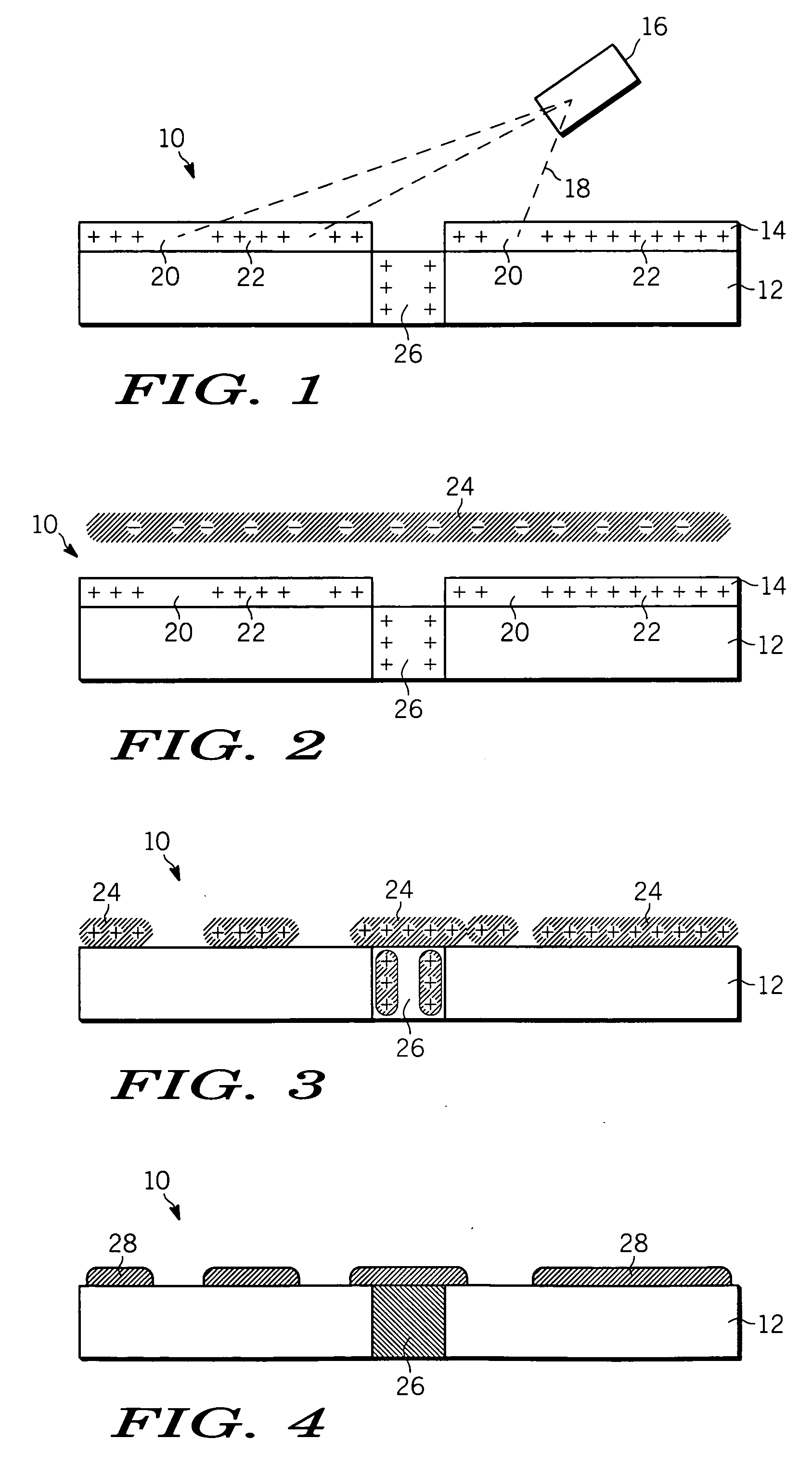
[0015] Referring now to FIG. 1, a cross-sectional view of a substrate 10 having a resin film 12 and an organic photo conductor (OPC) layer 14 in accordance with one embodiment of the present invention is shown. The substrate 10 may be formed from a sheet of insulator that is used to form the base of a PCB. The resin film 12, which is formed of a sticky substance like prepreg, may be laminated onto the substrate 10. The substrate 10 also includes at plurality of recesses 26. The OPC layer...


PUM

PropertyMeasurementUnit
Temperatureaaaaaaaaaa
Lengthaaaaaaaaaa

Abstract

A method for forming a metal layer on a substrate begins by providing a resin film on the substrate. An organic photo conductor layer having charged and uncharged segments is adhered to the resin film. Metal powder is deposited onto the charged segments of the organic photo conductor layer after which it is heated to form the metal layer.

Description

BACKGROUND OF THE INVENTION [0001] The present invention relates generally to printed circuit boards (PCBs). More particularly, the present invention relates to an apparatus and a method for fabricating a PCB without using wet chemicals. [0002] A printed circuit board (PCB) is a flat board or substrate, which is used to support semiconductor chips and other electronic components. The substrate includes a sheet of insulator or dielectric material having a number of conductive traces that are used to interconnect the electronic components. The traces are typically formed on the insulator by laminating a layer of copper foil over the substrate. A photoresist layer is formed on the copper foil. Excess copper is then removed from by chemical etching, leaving only the desired copper traces. Finally, electronic components may be soldered to the traces. [0003] The process may also be repeated to fabricate a multi-layer PCB, which comprises alternating layers of conductive and dielectric mat...

Claims


Application Information

Patent Timeline
IPC IPC(8): B05D1/12B05D5/12B01J19/08B29C71/04
CPCC23C24/10G03G13/28G03G13/283H05K2203/0517H05K3/1266H05K2203/0425H05K2203/043G03G13/286
Inventor SHIU, HEI MINGCHAU, ON LOKWONG, HO WANG
Owner FREESCALE SEMICON INC
Why Eureka
Try Eureka