Composite interconnect structure using injection molded solder technique

a technology of composite interconnect structure and solder, which is applied in the direction of non-conductive materials with dispersed conductive materials, metal/alloy conductors, and conductors. it can solve the problems of inability to form composite interconnect structures, difficult process, and particular interconnect structures that do not achieve all the possible advantages

Inactive Publication Date: 2007-08-02
GLOBALFOUNDRIES INC
View PDF30 Cites 13 Cited by
  • Summary
  • Abstract
  • Description
  • Claims
  • Application Information

AI Technical Summary

Benefits of technology

[0005] Composite interconnect structure forming methods using injection molded solder are disclosed. The methods provide a mold having at least one opening formed therein with each opening including a member of a material dissimilar to a solder to be used to fill the opening, and then fill the remainder of each opening with solder to form the composite interconnect structure. The resulting composite interconnect structure can be leveraged to achieve a much larger variety of composite structures than exhibited by the prior art. For example, the material may be chosen to be more electrically conductive than the solder portion, more electromigration-resistant than the solder portion and / or more fatigue-resistant than the solder portion. In one embodiment, the composite interconnect structure can include an optical structure, or plastic or ceramic material. The optical structure provides radiation propagation and / or amplification between waveguides in the substrate and device, and the plastic material provides fatigue-resistance.

Problems solved by technology

This reference, however, uses a very difficult process in which the composite interconnect structure is formed by cutting the material into bumps.
In addition, this particular interconnect structure does not achieve all of the possible advantages of composite interconnect structures.
This technique, however, is incapable of forming composite interconnect structures.

Method used


Image

  • Composite interconnect structure using injection molded solder technique
  • Composite interconnect structure using injection molded solder technique
  • Composite interconnect structure using injection molded solder technique

Examples


Embodiment Construction

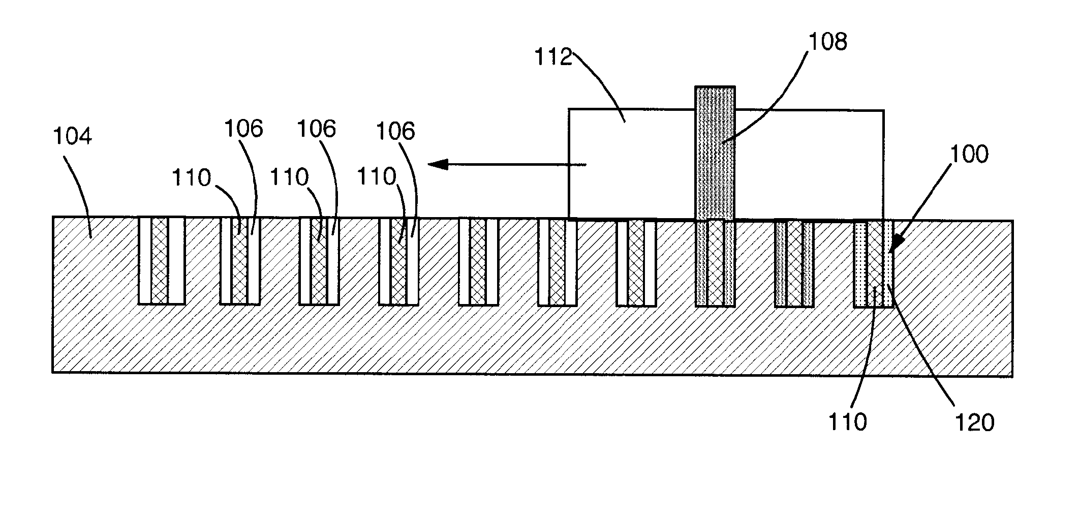
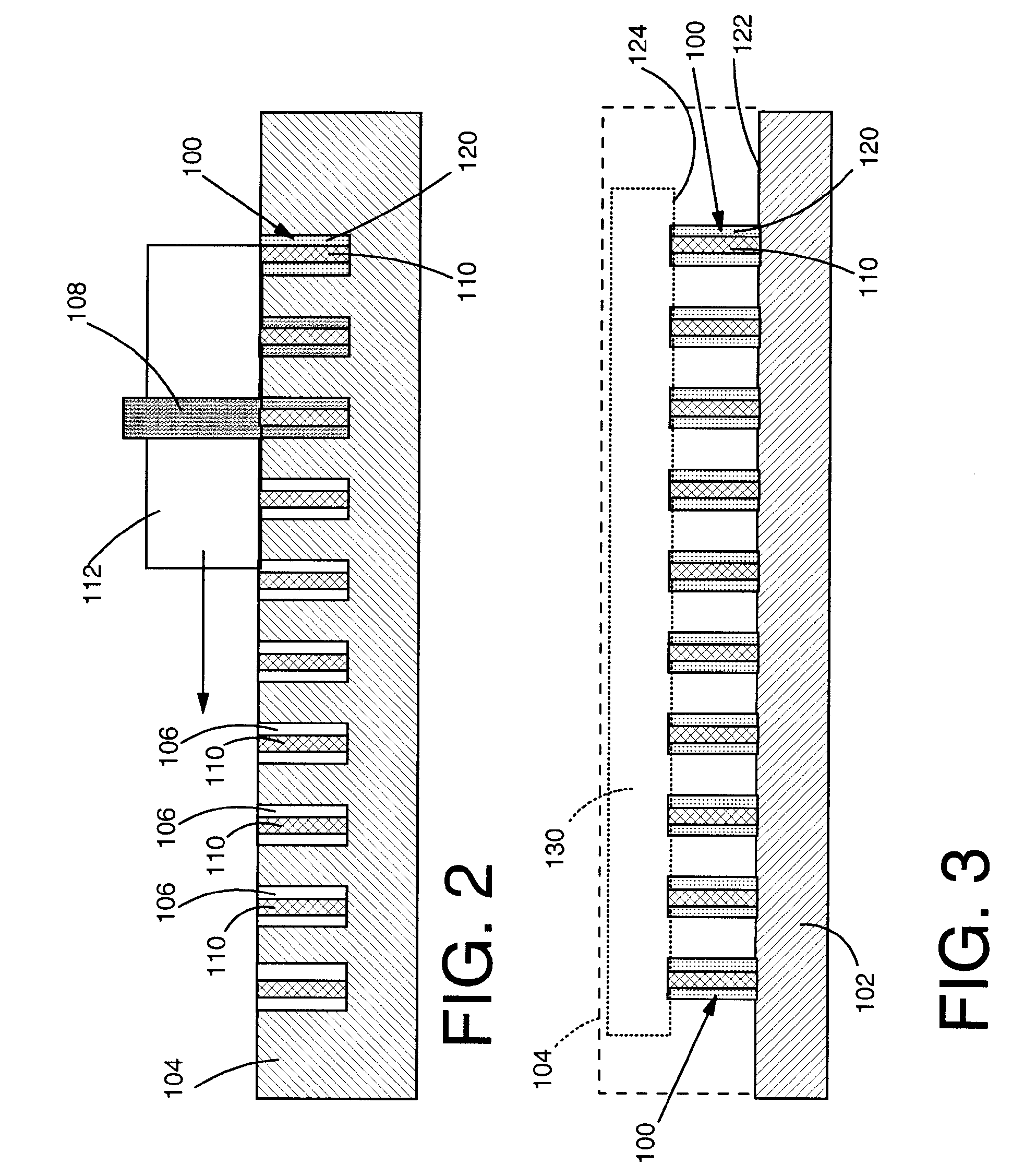
[0017] Turning to the drawings, FIGS. 2-3 show one embodiment of a method of forming a composite interconnect structure 100 on at least one of a substrate 102 (FIG. 3 only) and a semiconductor device 130 (FIG. 3 only) prior to packaging. In a first step, shown in FIG. 1, a mold 104 is provided having at least one opening 106 formed therein. As shown, mold 104 typically includes a plurality of openings 106. Each opening 106 includes a member 110 of a material dissimilar to a solder 108 (shown molten in FIG. 2) to be used to fill a remainder of each opening. Next, as also shown in FIG. 2, the remainder of each opening 106 is filled (injected) with a molten solder 108 using any now known or later developed molten solder injection device 112. As known to those with skill in the art, this step typically includes bringing molten solder injection device 112 into close proximity to mold 104 and injecting molten solder 108 into each opening 106. In this case, only the portion of each opening...


PUM

PropertyMeasurementUnit
oblong shapeaaaaaaaaaa
optical structureaaaaaaaaaa
electrical conductivityaaaaaaaaaa

Abstract

Composite interconnect structure forming methods using injection molded solder are disclosed. The methods provide a mold having at least one opening formed therein with each opening including a member of a material dissimilar to a solder to be used to fill the opening, and then fill the remainder of each opening with solder to form the composite interconnect structure. The resulting composite interconnect structure can be leveraged to achieve a much larger variety of composite structures than exhibited by the prior art. For example, the material may be chosen to be more electrically conductive than the solder portion, more electromigration-resistant than the solder portion and / or more fatigue-resistant than the solder portion. In one embodiment, the composite interconnect structure can include an optical structure, or plastic or ceramic material. The optical structure provides radiation propagation and / or amplification between waveguides in the substrate and device, and the plastic material provides fatigue-resistance.

Description

TECHNICAL FIELD [0001] The invention relates generally to interconnect structures, and more particularly, to a composite interconnect structure formed using injected molded solder. BACKGROUND ART [0002] Composite interconnect structures for coupling a semiconductor device to a substrate are advantageous for a number of reasons. For example, Japanese Patent Publication 7066209A discloses a composite interconnect structure including solder (e.g., gold-tin) with a core of a higher melting point than solder. The composite interconnect structure allows mounting of an optical device on a circuit board without tilting the devices, i.e., the core prevents a bump from compressing more than other bumps during mounting. This reference, however, uses a very difficult process in which the composite interconnect structure is formed by cutting the material into bumps. In addition, this particular interconnect structure does not achieve all of the possible advantages of composite interconnect struc...

Claims


Application Information

Patent Timeline
Patent Type & Authority Applications(United States)
IPC IPC(8): H01L21/00
CPCH01L21/4853H01L2224/11334H01L23/49811H01L24/11H01L24/12H01L24/16H01L24/742H01L2224/11003H01L2224/13099H01L2224/13147H01L2224/16H01L2924/01004H01L2924/01029H01L2924/01075H01L2924/01079H01L2924/09701H01L2924/01005H01L2924/01006H01L2924/01019H01L2924/01033H01L2924/014H01L21/6835H01L2224/05571H01L2224/05573H01L2924/00014H01L2224/05599
Inventor DANOVITCH, DAVID D.FAROOQ, MUKTA G.GAYNES, MICHAEL A.
Owner GLOBALFOUNDRIES INC
Why Eureka
Try Eureka