Semiconductor device and control method therefor

Active Publication Date: 2007-08-02
INFINEON TECH LLC
View PDF6 Cites 372 Cited by
  • Summary
  • Abstract
  • Description
  • Claims
  • Application Information

AI Technical Summary

Benefits of technology

[0009] According to a first aspect of the present invention, there is provided a semiconductor device including: a memory cell array comprising a plurality of nonvolatile memory cells; a detection circuit detecting the number of bits to be written as division data that is divided from data to be programmed into the memory cell array and comparing the number of bits with a predetermined number of bits; a latch circuit latching inversion data, which is either the division data inverted or not inverted in accordance with a result of comparing the number of bits with the predetermined number of bits; a write circuit coupled to the latch circuit and programming the inversion data into the memory cell array; and a control circuit coupled to the detection circuit, the latch circuit, and the write circuit to cause the detection circuit to detect the number of bits to be written as next division data and to compare the number of bits of the next division data with the predetermined number of bits, while concurrently controlling the write circuit to program the inversion data into the memory cell array. The division data is divided by the total number of bits to be written and needing a long programming time, and the division data is programmed, thereby shortening the programming time. In addition, while the write circuit is programming the inversion data from the latch circuit into the memory cell array, the detection circuit is detecting the number of bits to be written in the next division data and comparing the total number with a predetermined number. The programming time can be further shortened.
[0010] According to a second aspect of the present invention, there is provided a semiconductor device including: a memory cell array comprising a plurality of nonvolatile memory cells; a detection circuit detecting the number of bits to be written as division data that is divided from data to be programmed into the memory cell array and comparing the number of bits with a predetermined number of bits; a latch circuit latching inversion data, which is either the division data inverted or not inverted in accordance with a result of comparing the number of bits with the predetermined number of bits; and a write circuit coupled to the latch circuit and programming the inversion data into the memory cell array. The latch circuit may include a pair of nodes operating in a complementary manner, and latches the inversion data that is either the division data inverted or not inverted by inputting the division data into either of the pair of nodes in accordance with the result of comparing the number of bits with the predetermined number of bits. Data is input into the two nodes operating in a complementary manner, eliminating the necessity of the circuit to invert the division data, and reducing the circuit area.
[0011] According to a third aspect of the present invention, there is provided a semiconductor device including: a memory cell array comprising a plurality of nonvolatile memory cells; a read circuit reading division data that is divided from data to be read from the memory cell array; a control circuit determining whether index data indicates that the division data is inverted or not inverted when the division data is programmed; and a latch circuit latching the division data read by the read circuit and outputting inversion data that is either the division data inverted or not inverted in accordance with a result of determining whether the index data indicates that the division data is inverted or not inverted. The read circuit may read next division data from the memory cell array, while

Problems solved by technology

Consequently, in the operation of the virtual ground of flash memory with a NAND interface, it is difficult to program

Method used


Image

  • Semiconductor device and control method therefor
  • Semiconductor device and control method therefor
  • Semiconductor device and control method therefor

Examples


first embodiment

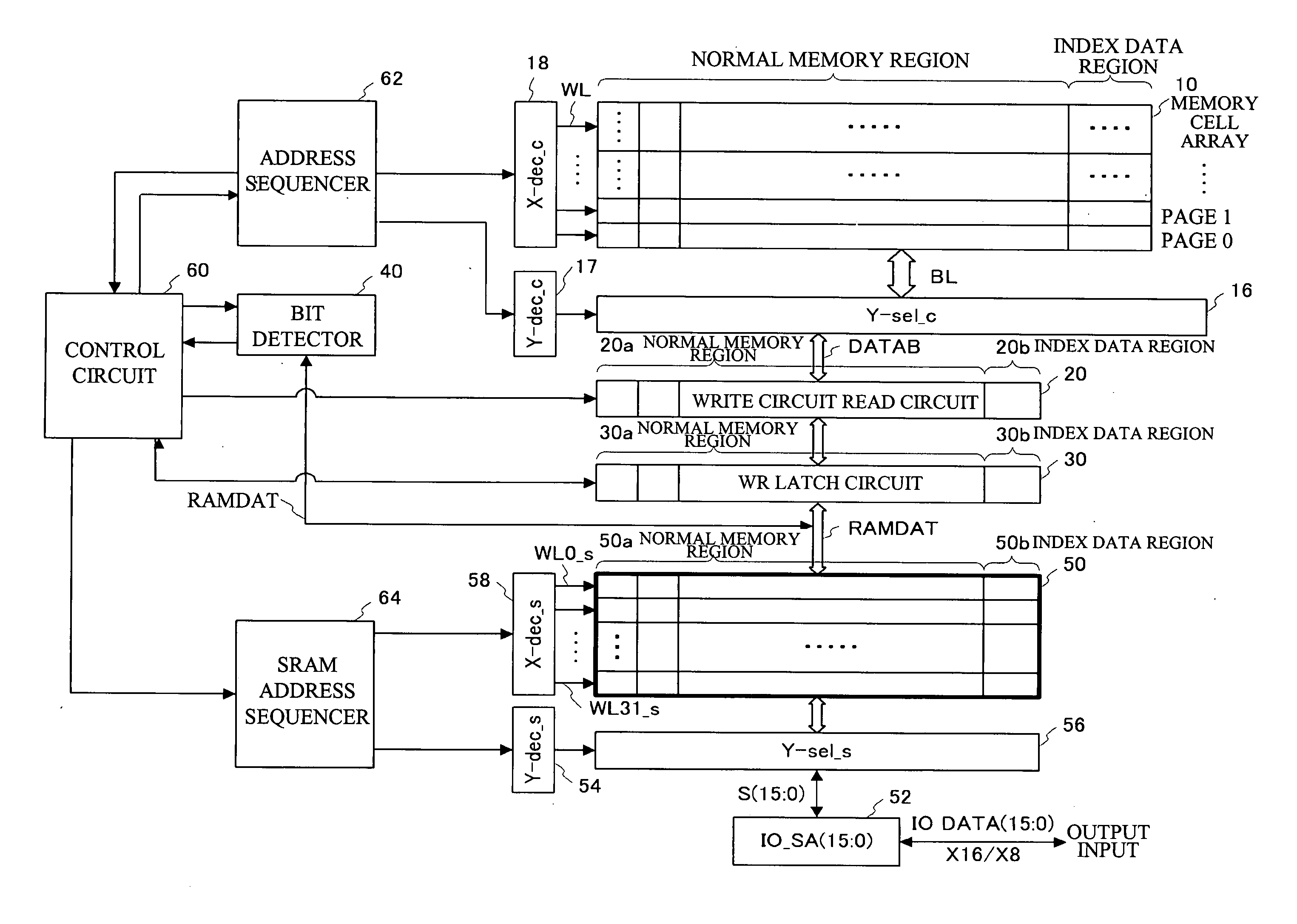
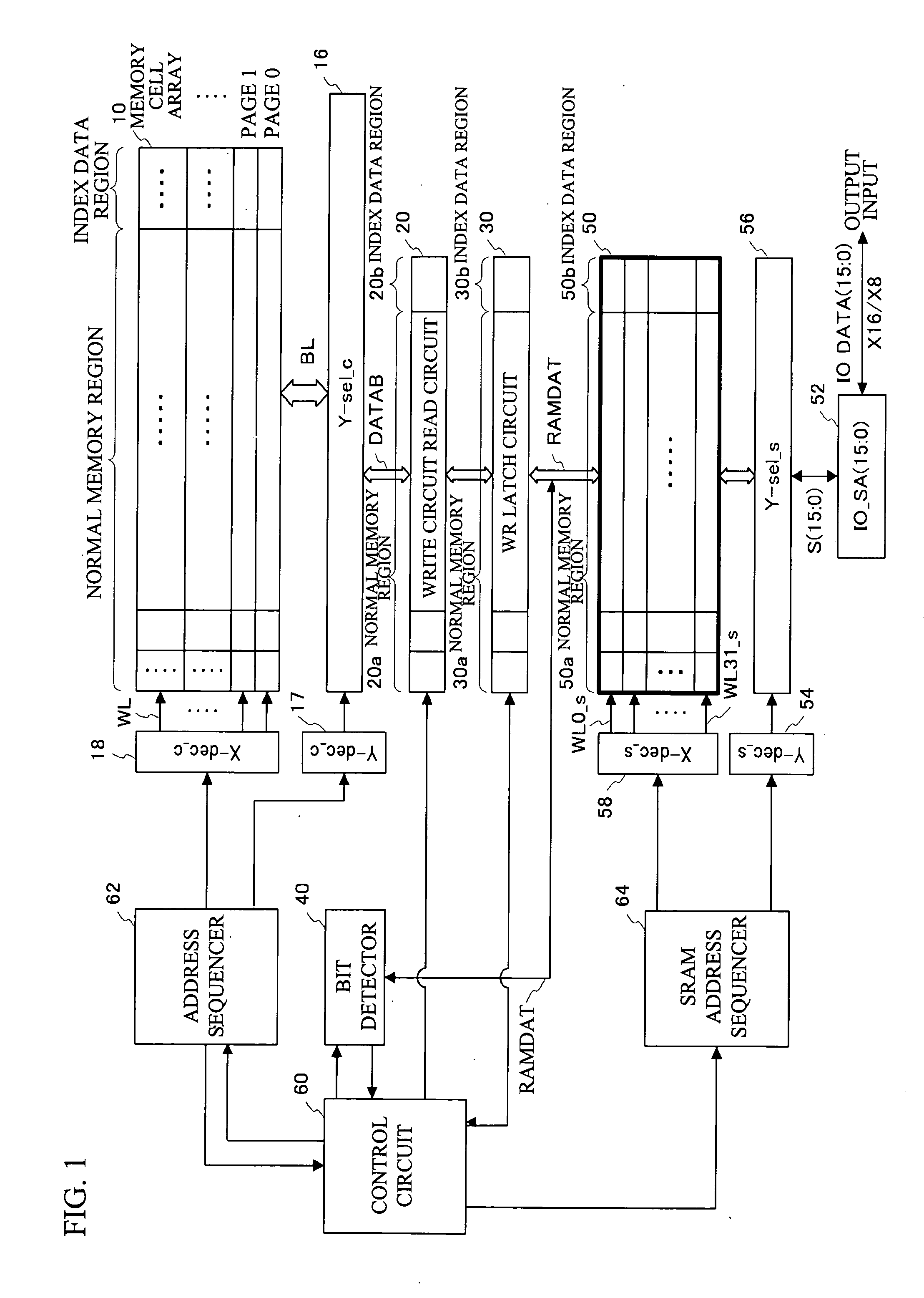
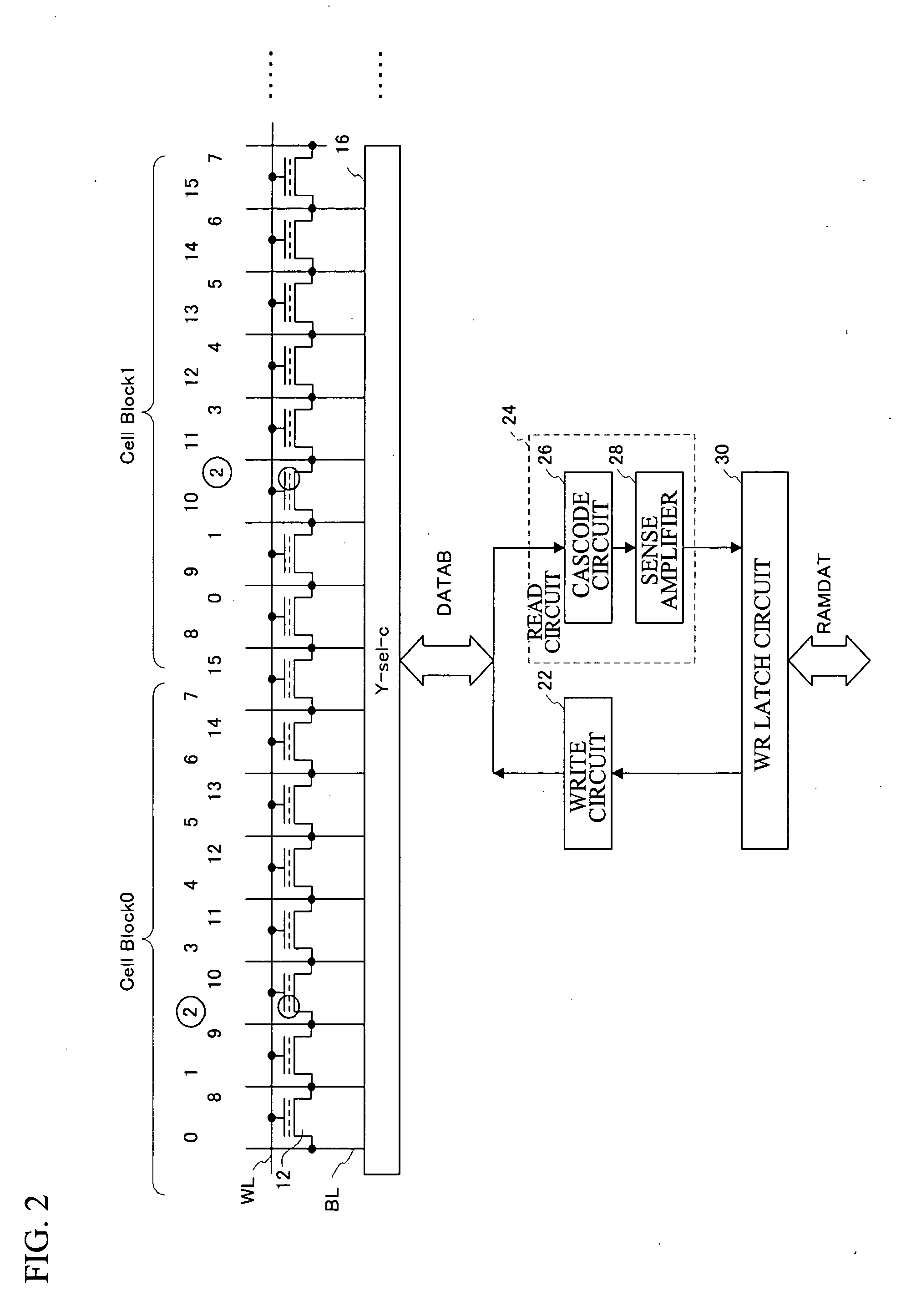
[0026] A first embodiment of the present invention is an example of a virtual ground flash memory having a NAND interface. The memory cells thereof are virtual ground nonvolatile memory cells, namely, SONOS flash memory cells in which a silicon nitride film serves as a charge storage layer. Two bits can be written into different charge storage regions in the charge storage layer. Hereinafter, “0” represents the state where the charge (electron) is stored in the charge storage region of the memory cell, and “1” represents the state where the charge (electron) is not stored therein. Hereinafter, making the memory cell “0” is referred to as write, and making the memory cell “0” or “1” is referred to as program.

[0027] In the flash memory employed in the first embodiment, input or output to or from the outside is performed through the NAND interface, and data is programmed or read on a page basis. In the first embodiment, data for one page is 2K Bytes, for example. The data, however, is...


PUM


Abstract

The present invention provides a semiconductor device and a method for controlling a semiconductor device having a memory cell array having a plurality of nonvolatile memory cells, the method including detecting the number of bits to be written as division data that is divided from data to be programmed into the memory cell array, comparing the number of bits with a predetermined number of bits, inverting or not inverting the division data to produce inversion data in accordance with a result of comparing the number of bits with the predetermined number of bits, and programming the inversion data into the memory cell array. The method further includes detecting the number of bits to be written as next division data and comparing the number of bits of next division data with the predetermined number of bits, while concurrently programming the inversion data into the memory cell array.

Description

CROSS-REFERENCES TO RELATED APPLICATIONS [0001] This is a continuation in part of International Application No. PCT / JP2005 / 022827, filed Dec. 13, 2005 which was not published in English under PCT Article 21(2).FIELD OF THE INVENTION [0002] Embodiments of the present invention relate generally to semiconductors and control methods therefor, and more particularly, to a semiconductor device having nonvolatile memory cells and a control method therefor. BACKGROUND OF THE INVENTION [0003] In recent years, nonvolatile memory semiconductor devices, in which data is rewritable, have been widely used. In a flash memory that is a typical nonvolatile memory, a transistor composing a memory cell has a floating gate or an insulation film known as charge storage layer. Data is stored by accumulating charges in the charge storage layer. [0004] In NAND flash memories, programming and reading are performed together on a page basis (for example, 2K Bytes). For this reason, there is provided a latch c...

Claims


Application Information

Patent Timeline
IPC IPC(8): G06F12/00
CPCG11C16/10G11C2207/2263
Inventor SAKASHITA, MOTOTADAYANO, MASARUOGAWA, AKIRANAKAI, TSUTOMU
Owner INFINEON TECH LLC
Why Eureka
Try Eureka