

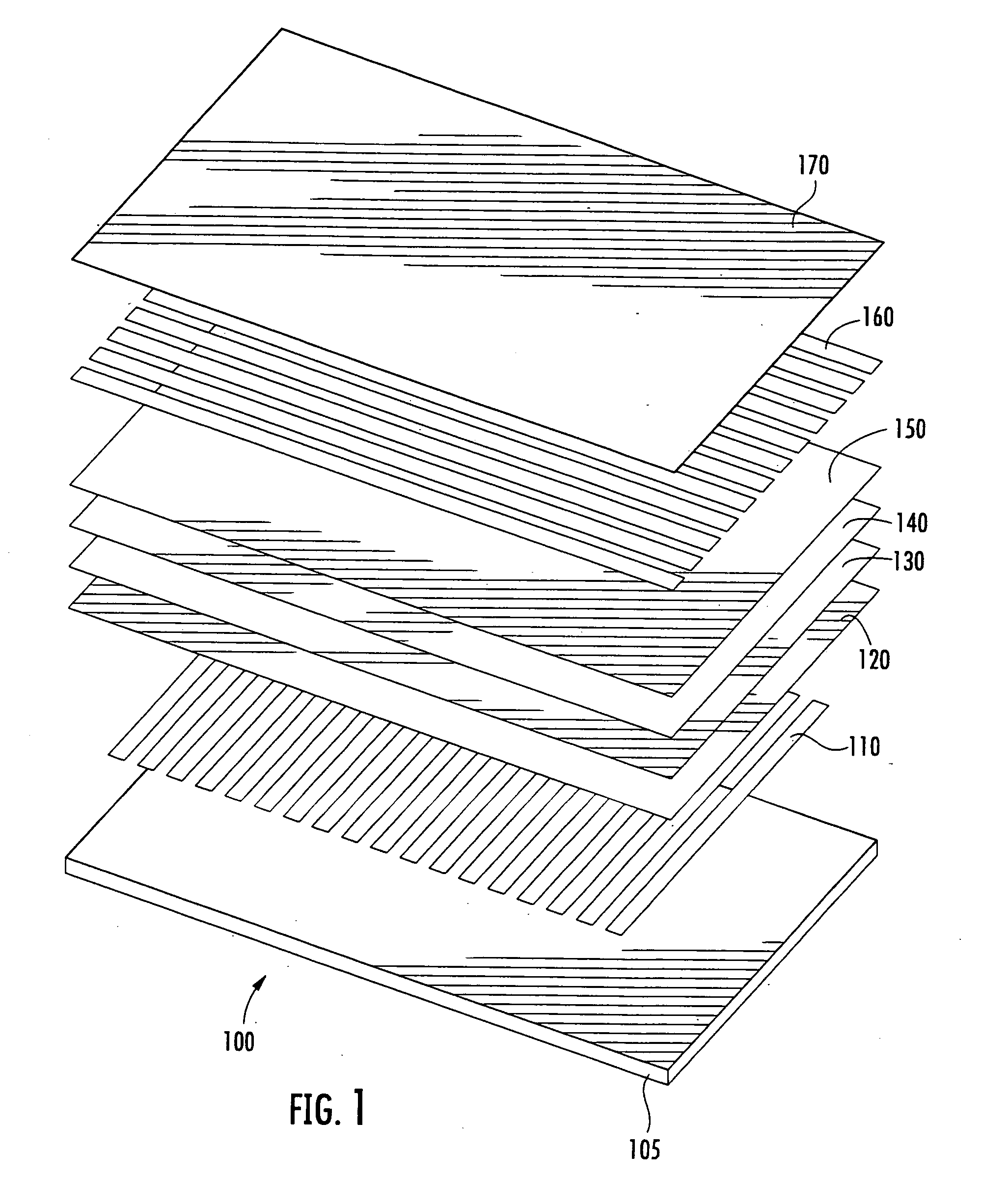
Charge transport layers and organic electron devices comprising same
a charge transport layer and electron transport technology, applied in the direction of discharge tube luminescnet screen, conductor, non-metal conductor, etc., can solve the problems of difficult multilayer deposition by solution processing, low conductivity of most hole transport or electron transport materials, and limited performance of charge injection and transport properties of these materials
- Summary
- Abstract
- Description
- Claims
- Application Information
AI Technical Summary
Benefits of technology
Problems solved by technology
Method used
Image

Examples
example 1
[0103] This example illustrates a p-doped hole injection material (or complex):
[0104] In the above case hole transport material m-OMTDATA is doped with electron deficient F4-TCNQ in a ratio of 2˜200:1 to form a p-doped hole injection material. The complex in various ratio will be tested for solubility in various solvents other than the common organic solvents for photoactive materials.
example 2
[0105] This example illustrates a n-doped electron injection material:
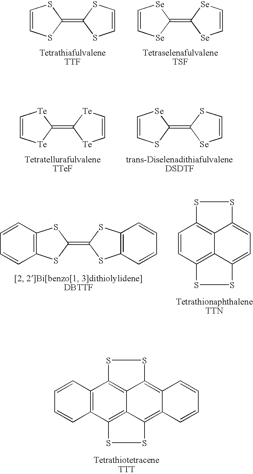
[0106] In the above case electron transport material FQP is doped with electron rich TTT in a ratio of 2˜200:1 to form a n-doped electron injection material. The complex in various ratio will be tested for solubility in various solvents other than the common organic solvents for photoactive materials.
example 3
[0107] This example illustrates a p-doped hole injection material. The hole injection material is a crosslinked polymer, P5 doped with C60.
(a) Synthesis of P5
[0108] This example demonstrates the preparation of hole transport material P5.
Synthesis of Compound 2
[0109] Under an atmosphere of nitrogen, a 250 mL round bottom was charged with 9,9-dioctyl-2,7-dibromofluorene (25.0 g, 45.58 mmol), phenylboronic acid (12.23 g, 100.28 mmol), Pd2(dba)3 (0.42 g, 0.46 mmol), PtBu3 (0.22 g, 1.09 mmol) and 100 mL toluene. The reaction mixture stirred for five minutes after which KF (8.74 g, 150.43 mmol) was added in two portions and the resulting solution was stirred at room temperature overnight. The mixture was diluted with 500 mL THF and filtered through a plug of silica and celite and the volatiles were removed from the filtrate under reduced pressure. The yellow oil was purified by flash column chromatography on silica gel using hexanes as eluent. The product was obtained as a white so...
PUM
| Property | Measurement | Unit |
|---|---|---|
| temperature | aaaaa | aaaaa |
| electrical energy | aaaaa | aaaaa |
| conductivity | aaaaa | aaaaa |
Abstract
Description
Claims
Application Information