Semiconductor component

a technology of semiconductor layers and components, applied in the direction of semiconductor devices, semiconductor/solid-state device details, electrical devices, etc., can solve the problems of component failure, thermal stress between the relatively sensitive semiconductor layer and the carrier body, and component sensitivity to changing temperatures during production process and operation

Inactive Publication Date: 2007-08-09
OSRAM OLED
View PDF10 Cites 39 Cited by
  • Summary
  • Abstract
  • Description
  • Claims
  • Application Information

AI Technical Summary

Benefits of technology

[0007] One object of the present invention is to provide a semiconductor component of the type mentioned in the introduction which reduces the thermal stresses between the semiconductor layer and the carrier body or substrate.
[0008] Another object of the invention is to provide a method for producing semiconductor components (including the type mentioned above but not restricted thereto) in which more rapid fabrication of the component and a more reliable end product are achieved.
[0012] The interspaces may advantageously be filled with a filling material that is more elastic than the carrier substrate material. This improves the stability of the component without impairing the ability of the patterned carrier substrate to absorb thermal stresses.
[0013] A further preferred embodiment has an individual vertical structure element that is arranged below the center of the semiconductor layer or element. This structure element serves as a stable core of the component and is limited in size in cross section parallel to the carrier base in such a way that thermal strains still do not lead to failures. The external space around the individual structure element is filled with a softer or more elastic material that can take up the thermal strains and additionally dissipate the heat from the semiconductor element.
[0014] In the above embodiments, the thermal stresses can additionally be reduced by selection of a carrier substrate material whose expansion coefficient is as close as possible to that of the semiconductor layer.
[0033] The production or the deposition of a mechanically stable carrier substrate on the adhesion and wetting layer in accordance with method step (d) is preferably carried out by means of a galvanic, method. This has the advantage that it is possible to compensate for small unevennesses in the surface of the wetting layer without constituting problems with adhesion.

Problems solved by technology

What is disadvantageous about components of this type is the sensitivity of the component to changing temperatures during the production process and during operation.
These lead to thermal stresses between the relatively sensitive semiconductor layer and the carrier body, which usually has a higher expansion coefficient than the semiconductor layer.
Such thermal stresses may cause cracks in the semiconductor, which leads to the failure of the component.

Method used


Image

  • Semiconductor component
  • Semiconductor component
  • Semiconductor component

Examples


Embodiment Construction

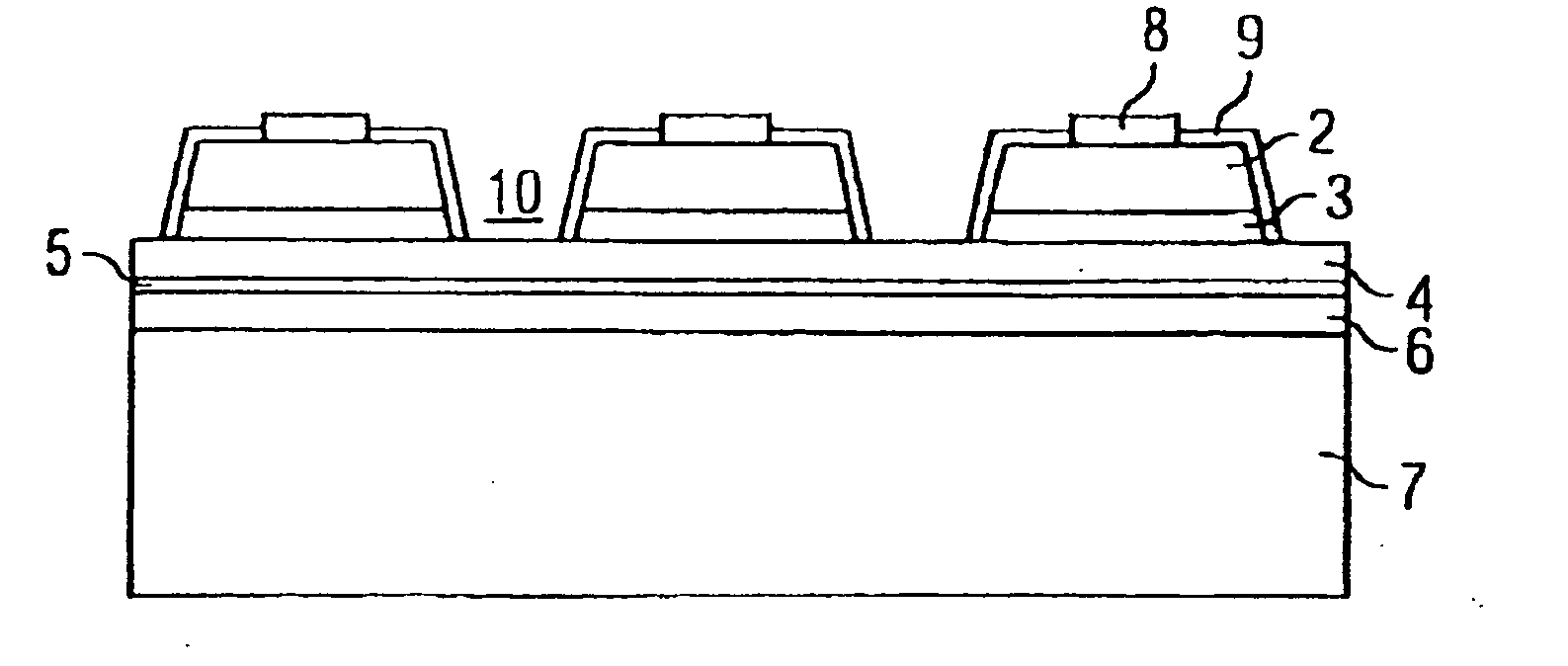
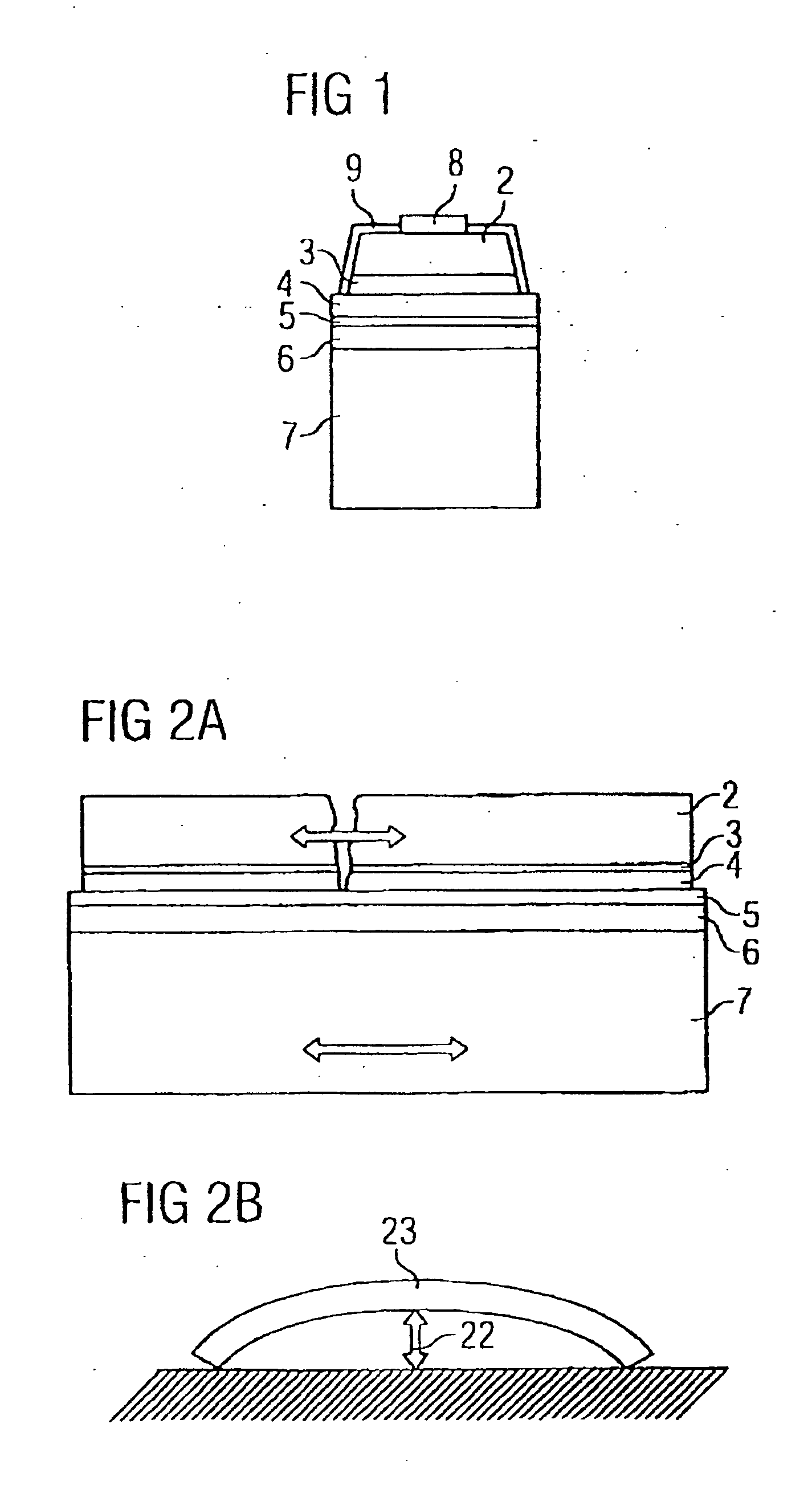
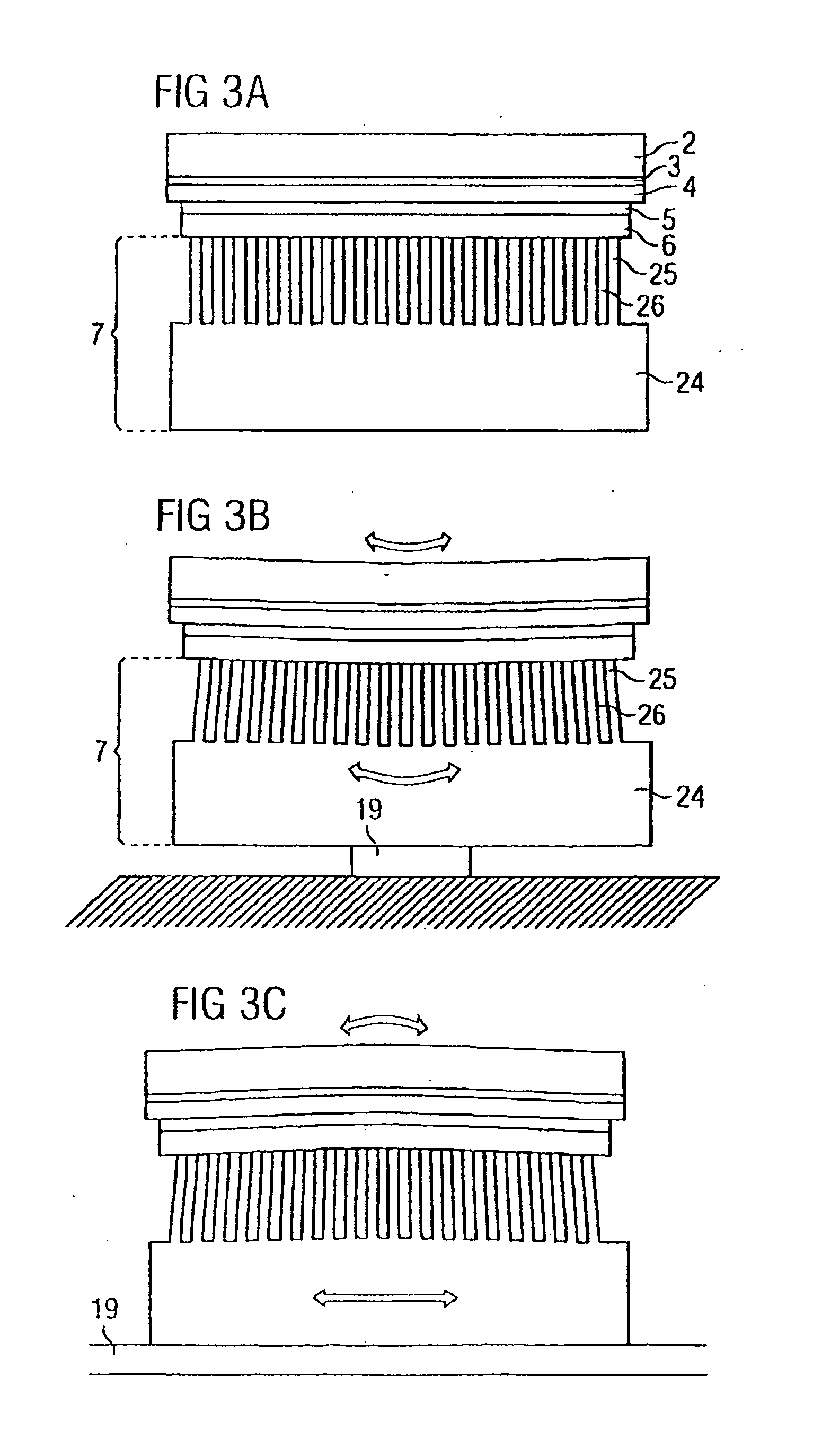
[0051] Identical or identically acting elements are provided with the same reference symbols in the figures. In particular the thickness of the layers is not illustrated to scale in the figures in order to afford a better understanding.

[0052] The semiconductor component illustrated in FIG. 1 has a semiconductor layer 2 arranged between a contact location 8 and a contact layer 3. The contact layer 3 may also be formed as an interrupted and / or patterned layer having a plurality of circular areas, by way of example. By way of example, the semiconductor layer 2 contains GaN and the contacts 3, 8 contain platinum, palladium or aluminum. The contact layer 3 (less than approximately 5 nm thick) lies on a reflection layer 4 (approximately 100 nm thick), which is very important for the light efficiency particularly in the case of optoelectronic applications. Depending on the light wavelength, the reflection layer 4 may comprise for example gold for the red spectral region or silver and alum...


PUM


Abstract

A semiconductor component having a light-emitting semiconductor layer or a light-emitting semiconductor element, two contact locations and a vertically or horizontally patterned carrier substrate, and a method for producing a semiconductor component are disclosed for the purpose of reducing or compensating for the thermal stresses in the component. The thermal stresses arise as a result of temperature changes during processing and during operation and on account of the different expansion coefficients of the semiconductor and carrier substrate. The carrier substrate is patterned in such a way that the thermal stresses are reduced or compensated for sufficiently to ensure that the component does not fail.

Description

CROSS-REFERENCE TO RELATED APPLICATIONS [0001] The present application is a divisional of application Ser. No. 10 / 529,673, filed Nov. 22, 2005; which is U.S. national stage of International Application No. PCT / DE2003 / 002954, filed Sep. 5, 2003. This patent application claims the priority of German patent Application No. 102 45 631.3, filed Sep. 30, 2002, the disclosure content of which is hereby incorporated by reference.BACKGROUND OF THE INVENTION [0002] 1. Field of the Invention [0003] The invention relates to a semiconductor component and a method for producing a semiconductor component having a light-emitting semiconductor layer or a light-emitting semiconductor element and two contact locations, which are formed as a contact layer and a contact. [0004] 2. Description of the Related Art [0005] Such a component is disclosed in published US Patent Application No. 2004 / 0099873, for example, which describes a semiconductor chip having contact locations on both sides and a reinforcin...

Claims


Application Information

Patent Timeline
Patent Type & Authority Applications(United States)
IPC IPC(8): H01L31/12H01L33/20
CPCH01L23/3677H01L33/20H01L2224/29164H01L2224/83203H01L24/83H01L2224/29169H01L24/29H01L24/95H01L2224/29014H01L2224/29124H01L2924/3512H01L2924/00H01L2924/351H01L2924/12042
Inventor EISERT, DOMINIKILLEK, STEFANSCHMID, WOLFGANG
Owner OSRAM OLED
Why Eureka
Try Eureka