Semiconductor device and manufacturing method thereof

a semiconductor and manufacturing method technology, applied in the field of semiconductor devices, can solve the problems of high cost, high cost, and high cost of polyimide resin tape, and achieve the effect of low cost of manufacturing semiconductor devices

Inactive Publication Date: 2007-08-09
MITSUI HIGH TEC INC
View PDF6 Cites 49 Cited by
  • Summary
  • Abstract
  • Description
  • Claims
  • Application Information

AI Technical Summary

Benefits of technology

[0010] The prevent invention has been devised in view of the above-described circumstances, and its object is to provide a method of manufacturing a semiconductor device which yields a small number of defectives by suppressing or eliminating the generation of plating burrs, as well as a semiconductor device manufactured by the same.
[0029] In the method of manufacturing a semiconductor device according to any one of the first to third aspects of the invention, since base metal plating or noble metal plating exhibiting etching solution resistance is provided as the lowermost layer of the plating mask, the generation of the plating burrs is maximally suppressed, and the deburring operation is not required. As a result, it is possible to provide a method of manufacturing a semiconductor device in which the fraction defective is low.
[0030] In addition, in the semiconductor device according to the fourth or fifth aspect of the invention, the connection terminal portions which are electrically connected to the electrode pad portions of the semiconductor element and the external connection terminal portions have their uppermost layers each constituted by a noble metal plating layer and their lowermost layers each constituted by base metal plating or noble metal plating exhibiting etching solution resistance. Therefore, it is possible to provide a semiconductor device in which the thickness of the plating is ensured, and the rate of defective products is low.
[0032] In addition, since special plating is not carried out in the formation of the plating mask, the cost of manufacturing semiconductor devices becomes low.

Problems solved by technology

However, the tape CSP type semiconductor devices have problems in that the polyimide resin tape is expensive, and that the polyimide resin tape is not suitable for strip transport since it is soft.
Meanwhile, the BCC type semiconductor devices have a problem in that after the base metal is removed by etching, discrete devices are left, so that their molded surfaces need to be fixed by pressure sensitive adhesive tape, resulting in high cost.

Method used


Image

  • Semiconductor device and manufacturing method thereof
  • Semiconductor device and manufacturing method thereof
  • Semiconductor device and manufacturing method thereof

Examples


first embodiment

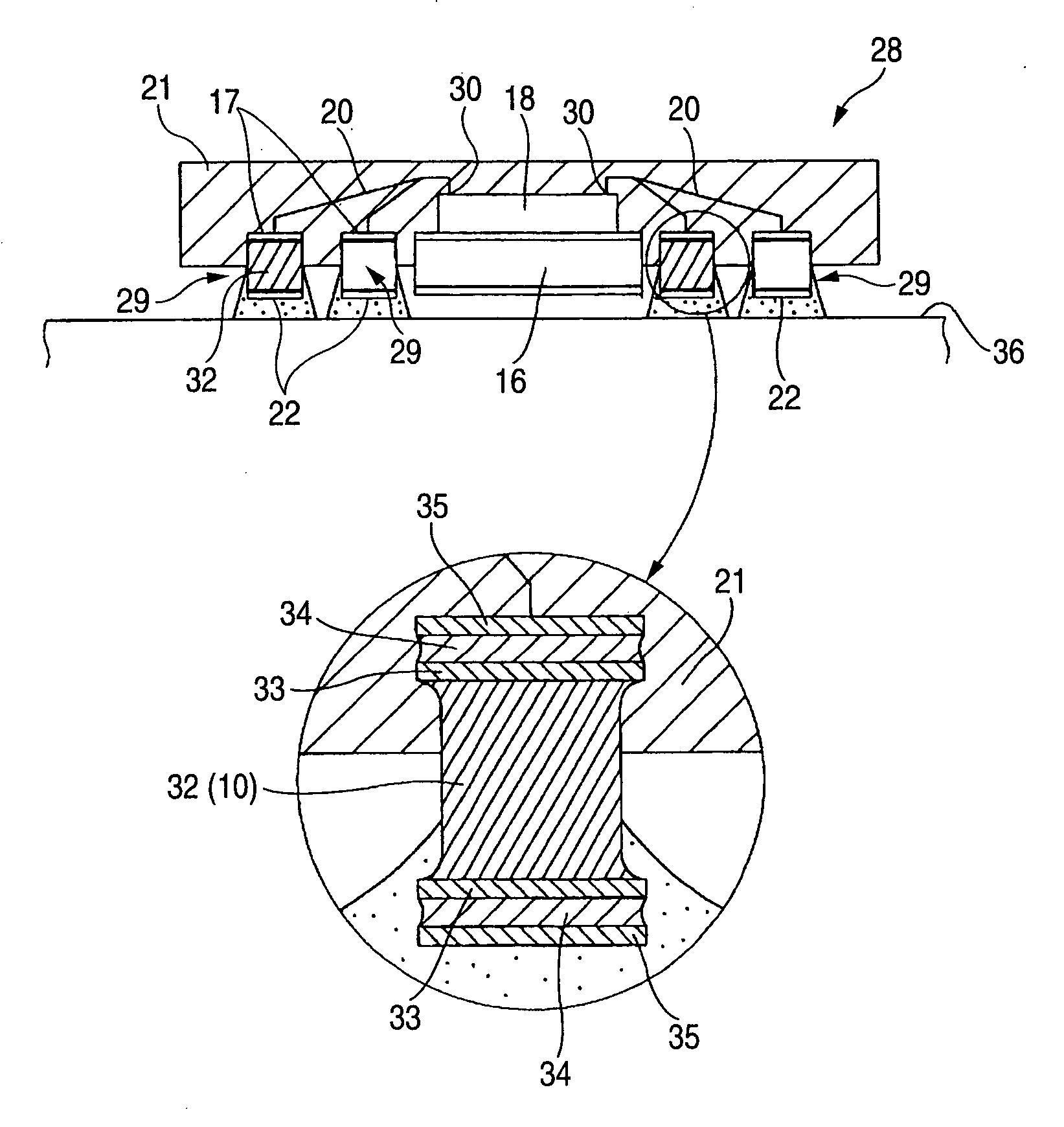
[0046] As shown in FIG. 1, the semiconductor device 28 in accordance with the invention has in its center a semiconductor element 18 and has in its periphery conductor terminals 29 whose upper surface sides (obverse surface sides) are formed as wire bonding portions 17 and whose lower surface sides (reverse surface sides) are formed as external connection terminal portions 22, the wire bonding portions 17 and the external connection terminal portions 22 being arranged in the form of area arrays. The wire bonding portions 17 and electrode pad portions 30 of the semiconductor element 18 are electrically connected by bonding wires 20, and upper halves of the semiconductor element 18, the bonding wires 20, and the conductor terminals 29 are resin encapsulated by an encapsulating resin 21.

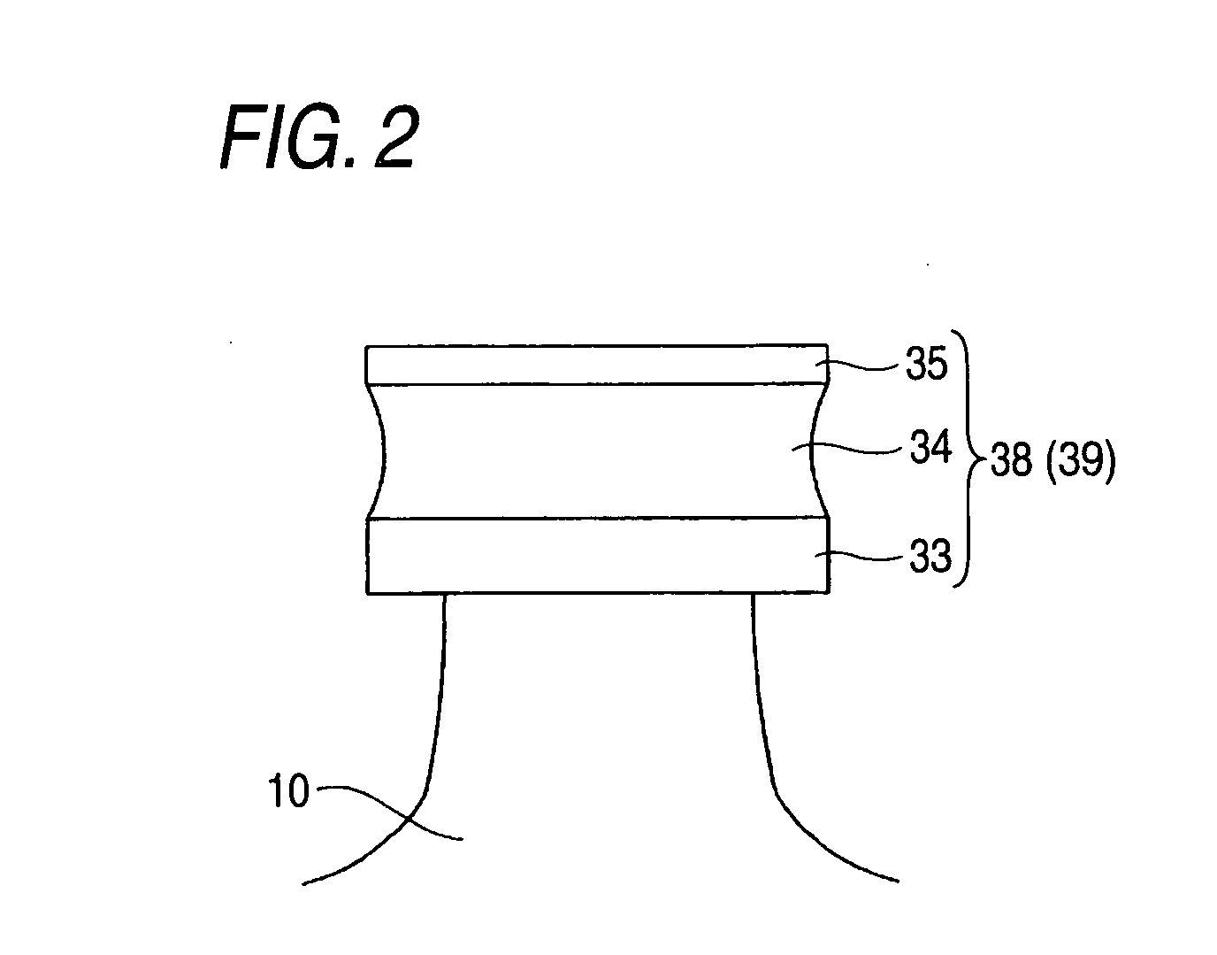
[0047] The details of the conductor terminal 29 are shown in FIG. 1. A gold plating 33 with a thickness of 0.15 to 0.5 μm, which is one example of noble metal plating exhibiting etching solution resista...

second embodiment

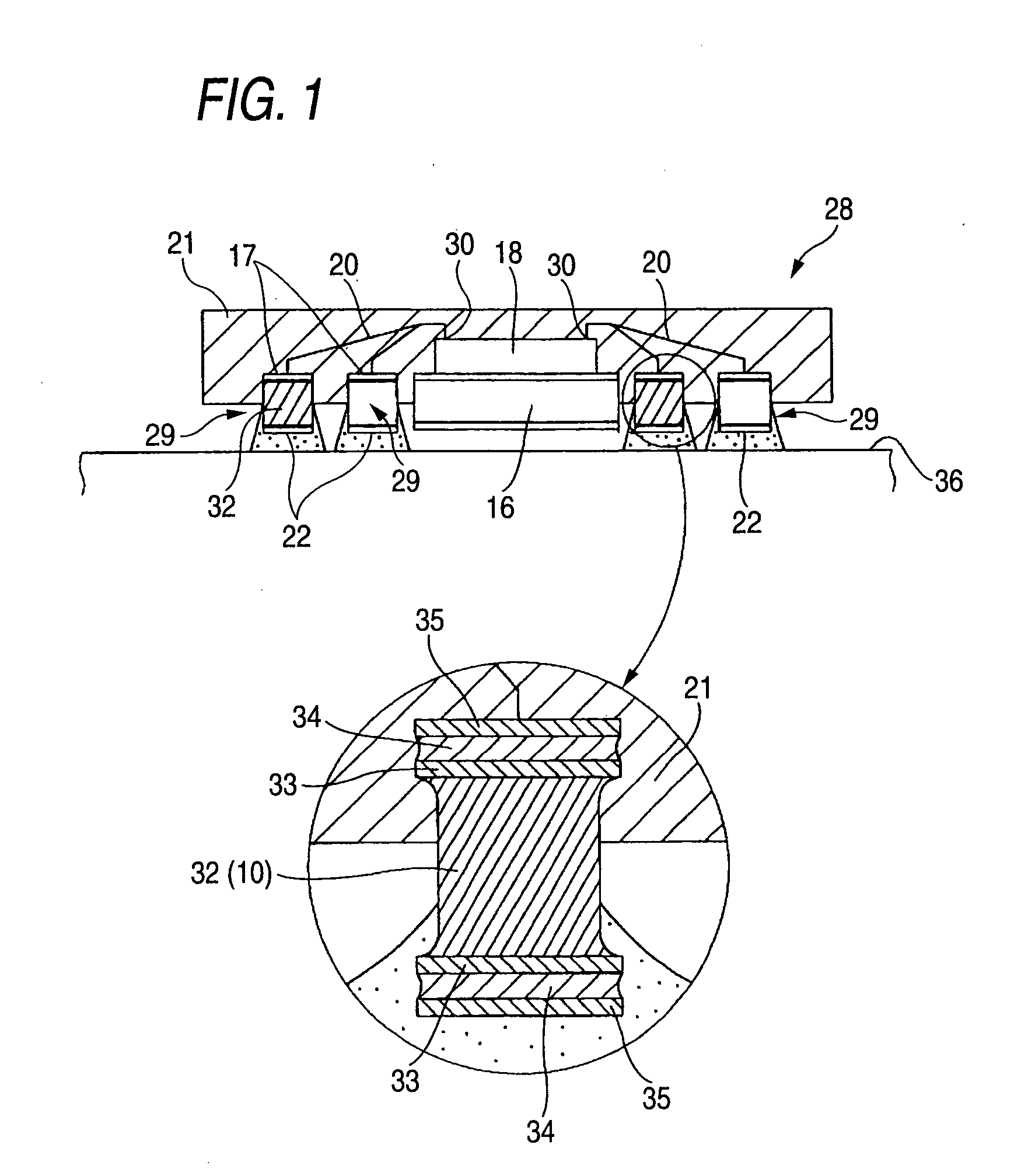
[0065] First, a description will be given of the semiconductor device 28 shown in FIG. 4 and manufactured by the method of manufacturing a semiconductor device in accordance with the invention. Those constituent elements which are identical to those of the method of manufacturing the semiconductor device shown in FIG. 1 are denoted by the same reference numerals, and a detailed description thereof will be omitted.

[0066] As shown in FIG. 4, the semiconductor device 28 manufactured by the method of manufacturing a semiconductor device in accordance with the second embodiment of the invention has in its center a semiconductor element 18 and has in its periphery the conductor terminals 29 whose upper surface sides (obverse surface sides) are formed as wire bonding portions 17, i.e., one example of the internal connection terminal portions, and whose lower surface sides (reverse surface sides) are formed as the external connection terminal portions 22, the wire bonding portions 17 and th...


PUM


Abstract

A method of manufacturing a semiconductor device 28 in which a plating mask 38, 39 having a noble metal plating layer 35 as an uppermost layer is formed at a predetermined portion on an obverse surface side or a reverse surface side of a leadframe material 10, and the leadframe material 10 is consecutively subjected to etching by using the plating mask 38, 39 as a resist mask, so as to form external connection terminal portions 22 which electrically communicate with a semiconductor element 18 disposed in an interior of an encapsulating resin 21, and which project downwardly. Base metal plating or noble metal plating 33 exhibiting etching solution resistance is provided as a lowermost layer of the plating mask 38, 39.

Description

BACKGROUND OF THE INVENTION [0001] The present invention relates to a semiconductor device of a chip size package type (hereinafter called as “CSP type”), and more particularly to a semiconductor device in which external connection terminal portions project from a bottom surface side of an encapsulating resin as well as a method of manufacturing the same. [0002] Tape CSP type semiconductor devices using polyimide resin tape and solder balls and bump chip carrier type (hereinafter called as “BCC type”) semiconductor devices using a base metal are known, reflecting demands for the miniaturization of semiconductor devices. However, the tape CSP type semiconductor devices have problems in that the polyimide resin tape is expensive, and that the polyimide resin tape is not suitable for strip transport since it is soft. Meanwhile, the BCC type semiconductor devices have a problem in that after the base metal is removed by etching, discrete devices are left, so that their molded surfaces n...

Claims


Application Information

Patent Timeline
Patent Type & Authority Applications(United States)
IPC IPC(8): H01L23/48H01L21/60
CPCH01L21/4832H01L2224/16245H01L23/3107H01L23/3114H01L23/49548H01L23/49582H01L24/48H01L24/81H01L24/85H01L2221/68377H01L2224/05599H01L2224/16H01L2224/48091H01L2224/48247H01L2224/484H01L2224/81801H01L2224/85439H01L2224/85444H01L2224/85447H01L2224/85464H01L2924/01004H01L2924/01005H01L2924/01028H01L2924/01029H01L2924/01033H01L2924/01046H01L2924/01047H01L2924/0105H01L2924/01078H01L2924/01079H01L2924/01082H01L2924/01083H01L2924/014H01L2924/15311H01L21/6835H01L2224/0401H01L2924/01006H01L2924/00014H01L2224/45099H01L2924/181H01L2924/18165H01L2924/00012H01L23/48
Inventor TAKAI, KEIJIHIRASHIMA, TETSUYUKI
Owner MITSUI HIGH TEC INC
Why Eureka
Try Eureka