Wafer surface inspection apparatus and wafer surface inspection method

a technology of surface inspection and wafer, which is applied in the direction of material analysis using wave/particle radiation, instruments, nuclear engineering, etc., can solve the problems of reducing the detection sensitivity, contaminating the wafer, and preventing the lowering of detection sensitivity, so as to increase the density of energy of irradiated laser

Active Publication Date: 2007-08-09
HITACHI HIGH-TECH CORP
View PDF9 Cites 2 Cited by
  • Summary
  • Abstract
  • Description
  • Claims
  • Application Information

AI Technical Summary

Benefits of technology

[0010] According to the present invention, irradiation of laser and spraying of gas with respect to the wafer are carried out at the same time and for the same location. This can increase the density of energy of irradiated laser at t

Problems solved by technology

However, it has become found that when the foreign particles are made of organic matter prone to break down, the foreign particles may be broken down (destructed) by heat of the laser irradiation, in which case the particles broken down would fly around the area and adhere to the wafer surface to thereby contaminate the wafer.
However, with an increase in sensitivity of detection of foreign particles, laser of high power

Method used


Image

  • Wafer surface inspection apparatus and wafer surface inspection method
  • Wafer surface inspection apparatus and wafer surface inspection method
  • Wafer surface inspection apparatus and wafer surface inspection method

Examples


Embodiment Construction

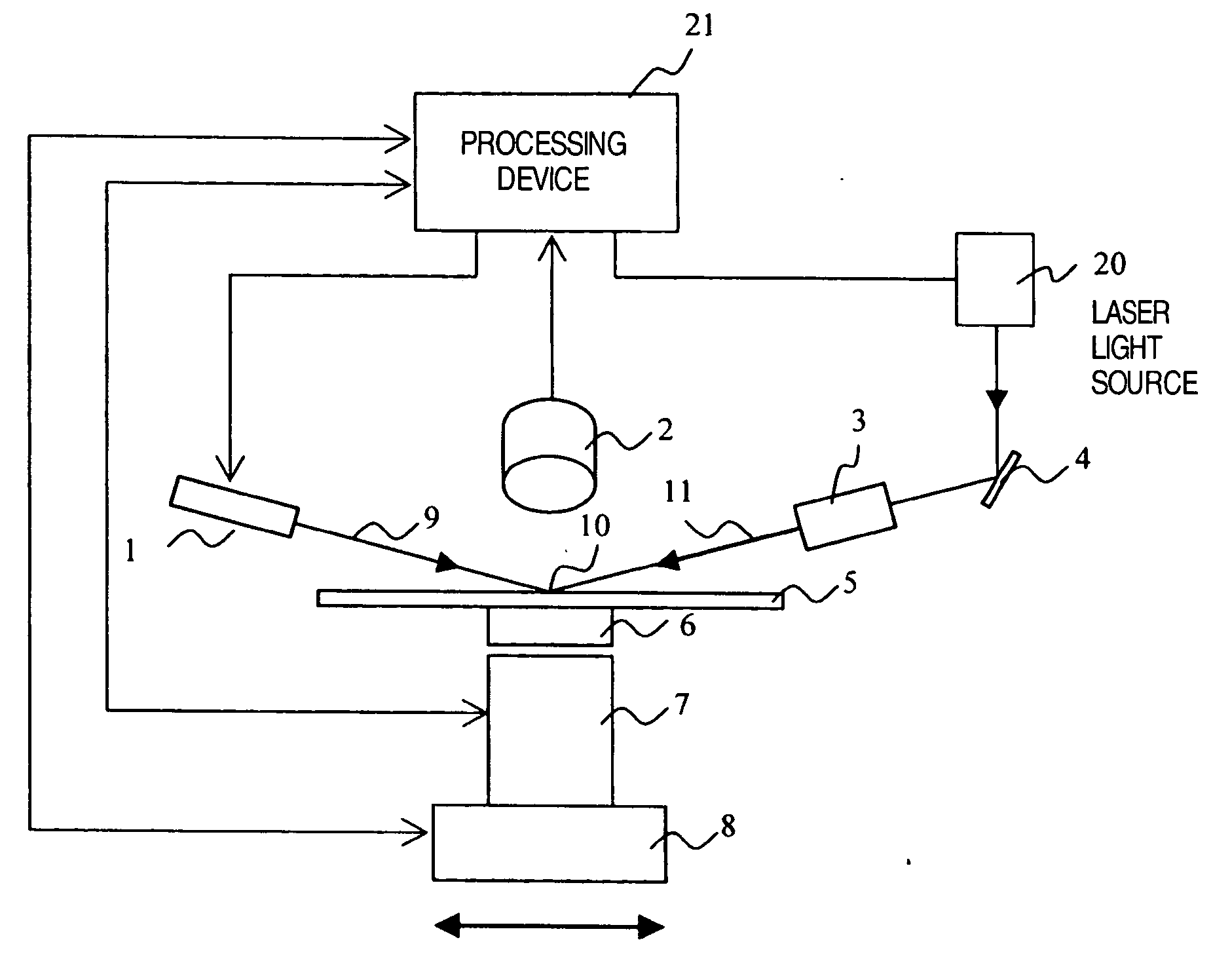
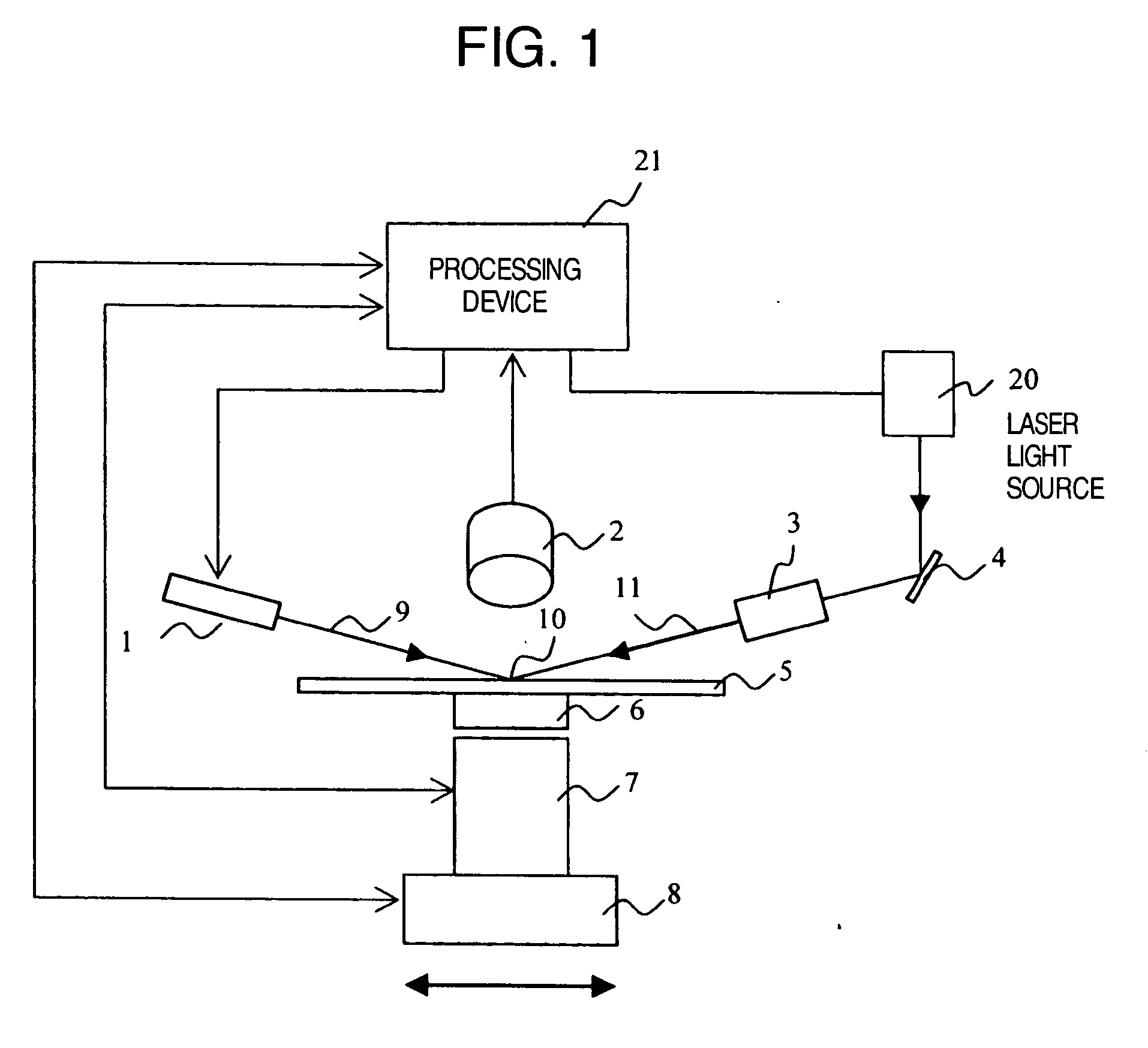
[0019] The inspection method and the inspection apparatus of the present invention are applicable to a flat plate-shaped subject to be inspected, such as a semiconductor wafer, a glass substrate for a liquid crystal panel, a disk substrate and the like. In the following, embodiments of the present invention will be described with reference to the drawings, taking a semiconductor wafer as an example.

[0020]FIG. 1 shows a schematic configuration of a foreign particle inspection apparatus of the present invention incorporating gas spraying means (gas spraying unit).

[0021] A semiconductor wafer 5 that is the subject to be inspected is rested on an inspection table 6, serving also as holding means (holder) or vacuum suction means (vacuum suction device), and is clamped or held with vacuum. A scanning stage 8 is mounted with an air spindle motor 7 to which inspection table 6 is attached, and is capable of generally horizontal movement backwards and forthwards in an axial direction. Air s...


PUM


Abstract

A wafer surface inspection method and apparatus of high sensitivity, and free from performance degradation in terms of cleanliness, coordinate repeatability of foreign particles and the like. Gas for cooling is sprayed onto a laser irradiation position on the wafer surface to prevent an increase in temperature of the foreign particles and to suppress break-down of the foreign particles.

Description

BACKGROUND OF THE INVENTION [0001] The present invention relates to a surface inspection apparatus and a surface inspection method of a subject to be inspected, and relates for example to a wafer surface inspection apparatus and a wafer surface inspection method for inspecting for foreign particles or foreign matter, defects and the like on a semiconductor wafer surface in a manufacturing process of a semiconductor device. [0002] In a manufacturing process of a semiconductor device, a circuit is formed by transferring a pattern onto a bare wafer and etching the same. In the manufacturing processes of various semiconductor devices during which circuits are formed, foreign particles adherent to the wafer surface, defects and the like become major factors causing a decrease in yield. The foreign particles adherent to the wafer surface and the defects are managed in each manufacturing process, and a wafer surface inspection apparatus detects the foreign particles adherent to the bare wa...

Claims


Application Information

Patent Timeline
IPC IPC(8): G01N21/88
CPCG01N21/94G01N2021/151G01N21/9501
Inventor ZAMA, KAZUHIROHACHIYA, MASAYUKI
Owner HITACHI HIGH-TECH CORP
Why Eureka
Try Eureka