Semiconductor device undergoing defect detection test

Inactive Publication Date: 2007-08-09
RENESAS ELECTRONICS CORP
View PDF3 Cites 4 Cited by
  • Summary
  • Abstract
  • Description
  • Claims
  • Application Information

AI Technical Summary

Benefits of technology

[0017]An object of the present invention is to provide a semiconductor device on which such a defect detection test as burn-in test can be performed appropriately.
[0020]In accordance with the present invention, such a defect detection test as burn-in test can be conducted appropriately.

Problems solved by technology

The initial failure refers to a failure occurring immediately after the start of use, due to deficiencies in device manufacturing process.
These defects relevant to tolerances that are failures becoming critical as the device is used belong to the initial failure.
The initial failure rate rapidly decreases with time, and subsequently the random failure period starts in which a low failure rate lasts for a certain long period.
Then, the wear-out failure period starts in which the end of useful life of the device is being reached and the failure rate sharply increases.
In the case where the memory cell stores H data (data having a logically high level) and the access transistor is OFF for example, application of the same voltage as H data to the gate of the access transistor could be insufficient to cause electric charges stored in the memory cell capacitor to flow out from the gate, resulting in flow of off-leakage current.
This is a problem for a thin film transistor having a small gate voltage for turning the transistor ON.
Furthermore, since the external power supply voltage in burn-in test is larger than that in normal operation as described above, further excessive stress is imposed on the transistor, which could cause the gate oxide film of the transistor to be broken.
However, no measures are taken to address malfunctions due to a larger voltage difference between two voltages supplied to a memory cell or the like.
However, no measures are taken to address malfunctions due to a voltage difference between two voltages supplied to a memory cell or the like.
Thus, high electric field stress cannot be applied to the device, resulting in the problem that the burn-in test takes a long time.
In addition, since the external power supply voltage cannot be increased, stress for revealing initial failures cannot be applied to the gate oxide film for example of the transistor, resulting in the problem that initial defectives cannot be removed sufficiently.
However, a pad for applying a power supply voltage except for the external power supply voltage for normal operation has to be provided, which could increase the circuit size and area.

Method used


Image

  • Semiconductor device undergoing defect detection test
  • Semiconductor device undergoing defect detection test
  • Semiconductor device undergoing defect detection test

Examples


first embodiment

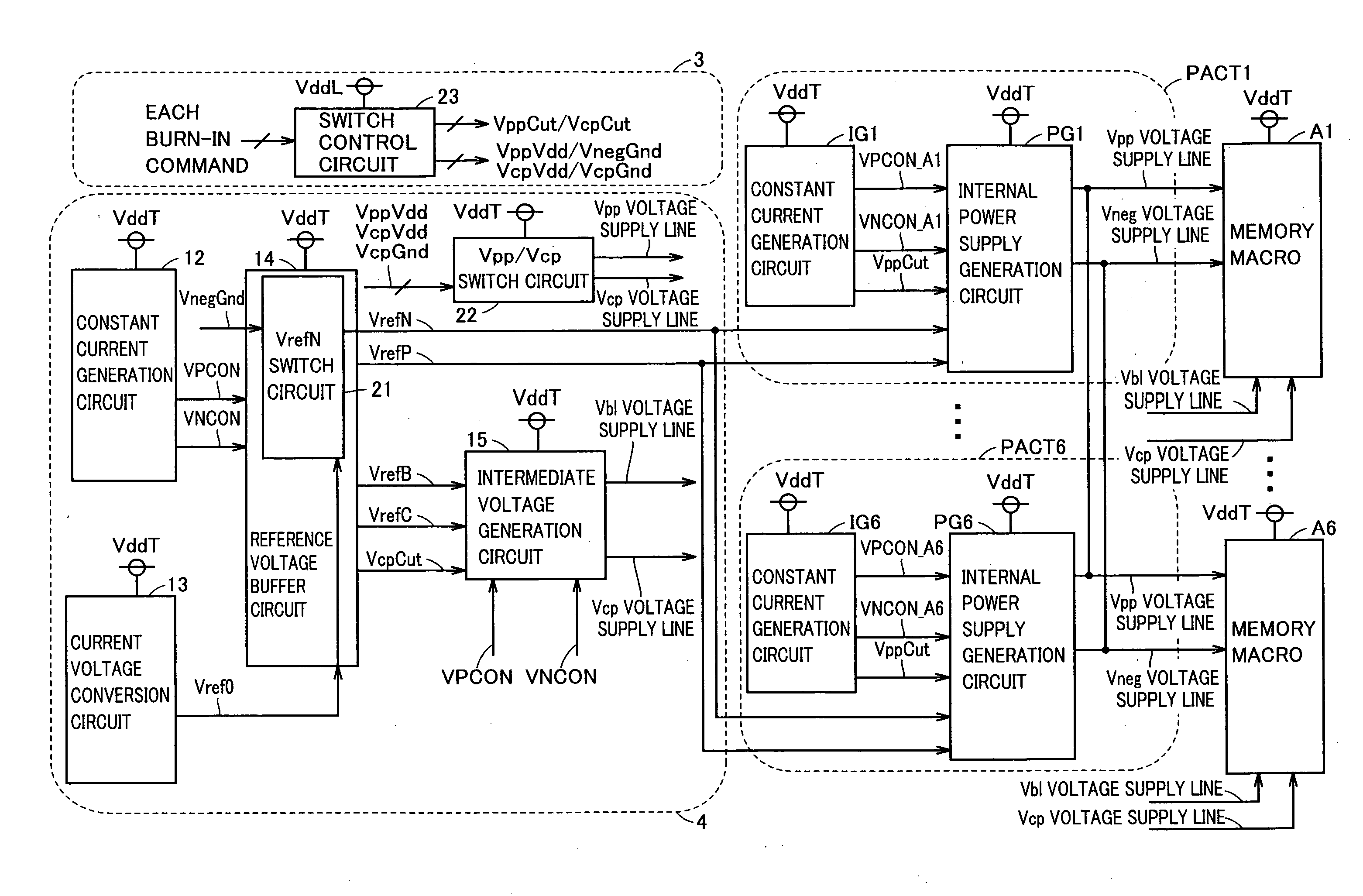
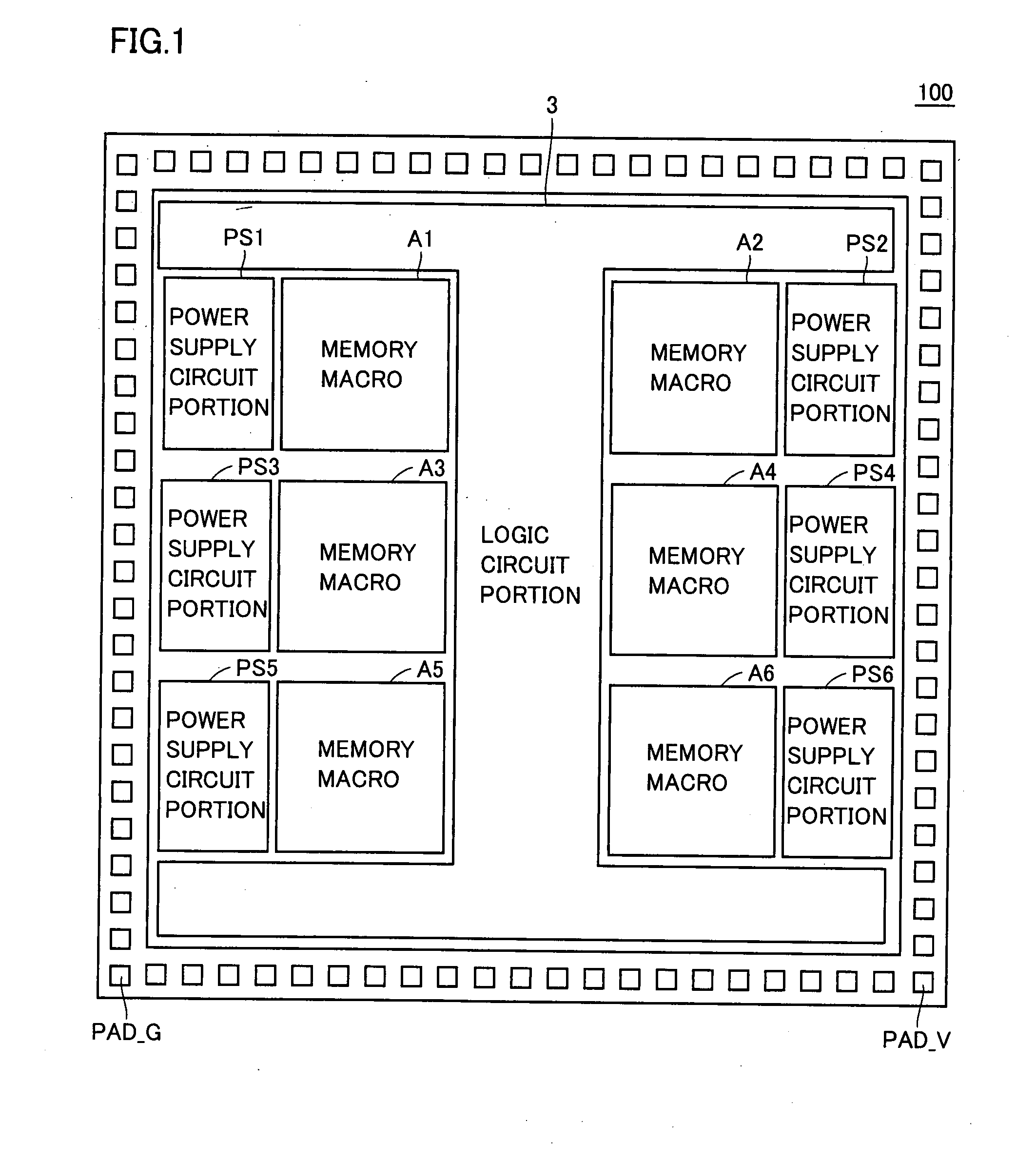
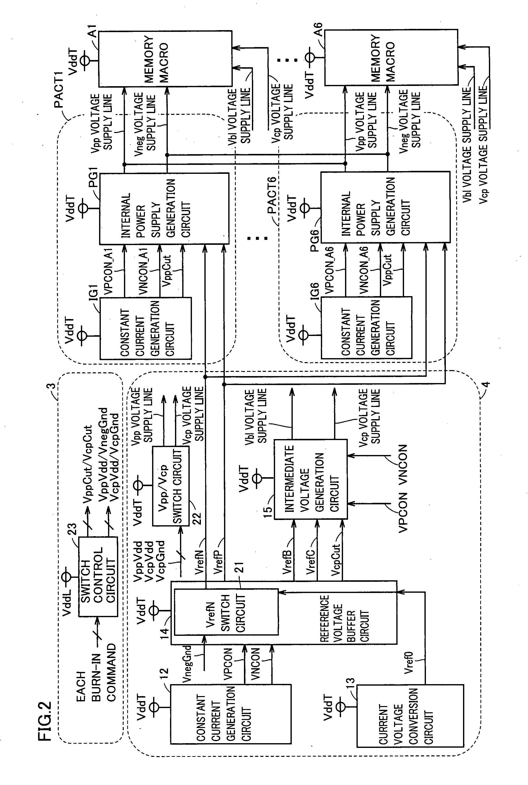
[0055]FIG. 1 schematically shows an arrangement of a semiconductor device according to a first embodiment of the present invention.

[0056]Referring to FIG. 1, the semiconductor device is a logic-merged memory for example and includes a logic circuit portion 3, memory macros (memory portions) A1 to A6 and power supply circuit portions PS1 to PS6. Logic circuit portion 3, memory macros A1 to A6 and power supply circuit portions PS1 to PS6 are arranged on the same chip. Around logic circuit portion 3, memory macros A1 to A6 and power supply circuit portions PS1 to PS6, pads are successively arranged for externally supplying power from the outside of the semiconductor device. For example, external power supply voltage VddT and ground voltage GND are supplied via pad PAD_V and pad PAD_G to the semiconductor device.

[0057]The semiconductor device has a first operation mode corresponding to normal operation in which data is externally written to and read from the semiconductor device, and a ...

second embodiment

[0156]The present embodiment relates to a semiconductor device in which the voltage supplied to the negative voltage supply line in burn-in test is changed, as compared with the semiconductor device of the first embodiment. The configuration and operation of the semiconductor device, except for the features described below, are similar to those of the semiconductor device of the first embodiment.

[0157]FIG. 16 shows a configuration of a Vneg burn-in circuit and its peripheral circuits according to the second embodiment of the present invention.

[0158]Referring to FIG. 16, Vneg burn-in circuit 51_N includes a VrefN switch circuit 21 and a VrefN switch control circuit 23_N. VrefN switch control circuit 23_N is provided within logic circuit portion 3. Power supply circuit portions PS1 to PS6 include Vneg internal power supply generation circuits PG1_N to PG6_N, and only power supply circuit portion PS1 includes a reference voltage buffer circuit 14. Reference voltage buffer circuit 14 in...

third embodiment

[0200]The present embodiment relates to a semiconductor device additionally having the pump-number changing function as compared with the semiconductor device of the second embodiment. The configuration and operation of the semiconductor device, except for the features described below, are similar to those of the semiconductor device of the second embodiment.

[0201]FIG. 21 schematically shows a configuration of a Vneg burn-in circuit having the pump-number changing function according to the third embodiment of the present invention.

[0202]Referring to FIG. 21, Vneg burn-in circuit 51_NP having the pump-number changing function includes a VrefN switch circuit 21 and a VrefN switch control circuit 23_NP.

[0203]VrefN switch control circuit 23_NP outputs, based on the Vneg burn-in command and the Vneg cut command, burn-in signal VnegGnd, cut signal VnegCut and cut signal VnegCut_BI.

[0204]Vneg voltage supply lines driven respectively by Vneg internal power supply generation circuits PG1_N t...


PUM


Abstract

A semiconductor device has a first operation mode and a second operation mode in which power supply with a higher voltage value than that in the first operation mode is provided. The semiconductor device includes a memory portion having memory cells for storing data and a power supply circuit portion supplying a first voltage and a second voltage to the memory portion. The memory portion writes or reads data to or from the memory cells based on the first voltage and the second voltage, and the power supply circuit portion provides a smaller voltage difference between the first voltage and the second voltage in the second operation mode as compared with the voltage difference in the first operation mode.

Description

BACKGROUND OF THE INVENTION[0001]1. Field of the Invention[0002]The present invention relates to a semiconductor device, particularly to a semiconductor device on which a defect detection test is performed.[0003]2. Description of the Background Art[0004]Due to the recent progress in semiconductor manufacturing technology, a logic-merged memory has been implemented that has, on the same chip, a logic circuit and a memory and data can be communicated between the logic circuit and the memory. Since such a logic-merged memory can have an improved transfer rate between the logic circuit and the memory, high-speed data processing can be achieved.[0005]In the logic-merged memory, in terms of high-speed operation and power consumption for example, a memory cell configured with a thin-film transistor for logic applications that can provide high performance with a low voltage is used. As for the memory cell structure, a so-called twin cell structure comprised of, for example, two MOS transist...

Claims


Application Information

Patent Timeline
IPC IPC(8): G11C29/00G11C11/34G11C16/04G11C7/00G11C16/06
CPCG11C29/12G11C29/12005G11C29/48
Inventor YOSHINAGA, KENJIMATSUMURA, MASASHIIGAUE, FUTOSHIAKIYAMA, MIHOKOMORISHITA, FUKASHI
Owner RENESAS ELECTRONICS CORP
Why Eureka
Try Eureka