Devices including graphene layers epitaxially grown on single crystal substrates

a technology of graphene and substrate, applied in the field of electromechanical devices, can solve the problems of graphite having a relatively large lattice-mismatch of about 20%, growing single sheets of graphene, and the most vulnerable monolayer of carbon to damag

Active Publication Date: 2007-08-16
ALCATEL-LUCENT USA INC +1
View PDF12 Cites 160 Cited by
  • Summary
  • Abstract
  • Description
  • Claims
  • Application Information

AI Technical Summary

Benefits of technology

[0012] In accordance with one aspect of my invention, an electronic device comprises a body including a single crystal region on a major surface of the body, the region having a hexagonal crystal lattice that is substantially lattice-matched to graphene, and at least one epitaxial layer of graphene disposed on the region. In a currently preferred embodiment, the single crystal surface region comprises multi-layered hexagonal BN, which has the requisite hexagonal crystal lattice within each layer and has less than about a 2% lattice mismatch to graphene. In addition, it is also preferred that only a single layer of graphene is disposed on the region. In accordance with another aspect of my invention, a method of making an electronic device comprises the steps of: (a) providing a body including a single crystal region on a major surface of the body, the region having a hexagonal crystal lattice that is substantially lattice-matched to graphene, and (b) epitaxially forming at least one graphene layer on that region. In a currently preferred embodiment, step (a) further includes the steps of (a1) providing a single crystal substrate of graphite and (a2) epitaxially forming single crystal hexagonal BN on the substrate. The hexagonal BN has a surface region, which has a multi-layered, hexagonal crystal lattice within each layer and is substantially lattice-matched to graphene, and step (b) includes epitaxially forming the graphene layer on the hexagonal BN surface region.

Problems solved by technology

Growing single sheets of graphene, however, remains a problem, according to Wilson the monolayers of carbon are most vulnerable to damage when being heated during typical fabrication processes.
In fact, SiC and graphite have a relatively large lattice-mismatch of about 20%, which is typically much too large for depositing device-quality epitaxial graphite layers on a SiC substrate.

Method used


Image

  • Devices including graphene layers epitaxially grown on single crystal substrates
  • Devices including graphene layers epitaxially grown on single crystal substrates
  • Devices including graphene layers epitaxially grown on single crystal substrates

Examples


Embodiment Construction

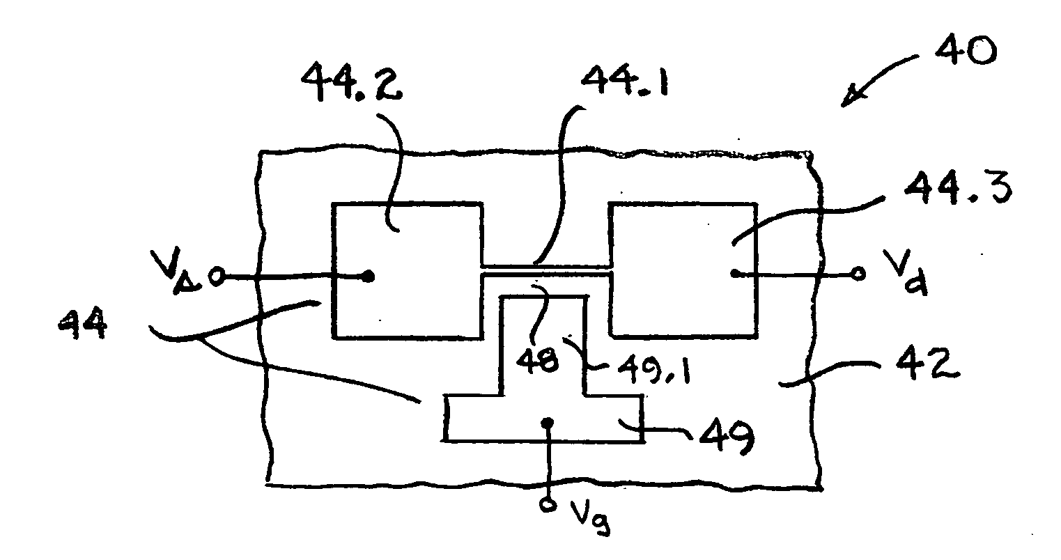
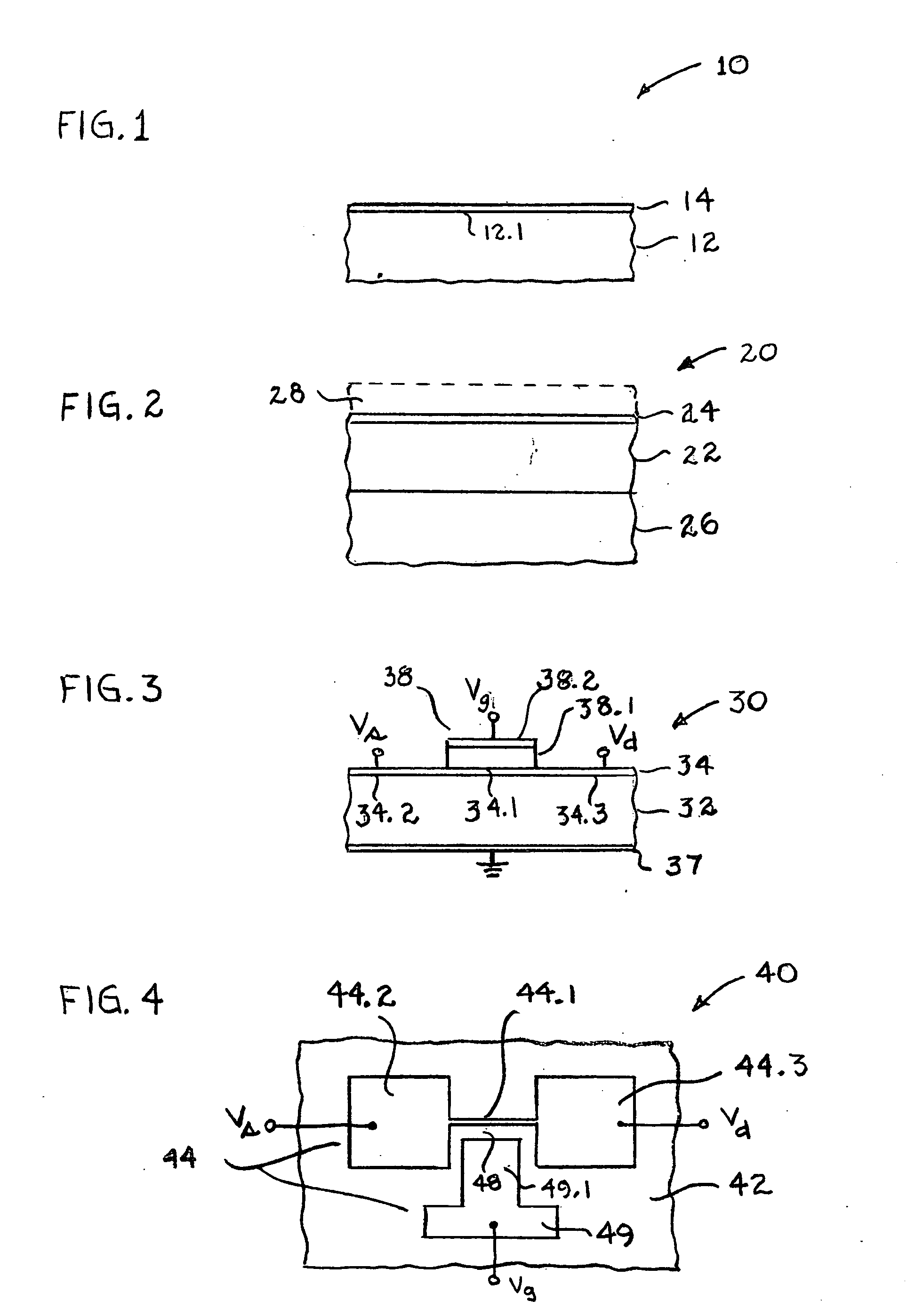
[0021] With reference now to FIG. 1, an electronic device 10 comprises a body 12 having a single crystal region 12.1 on a major surface of the body 12. The region 12.1 has a hexagonal crystal lattice that is substantially lattice-matched to graphene, and at least one layer 14 of graphene epitaxially disposed on region 12.1. Preferably, only a single layer of graphene is formed on region 12.1. A single graphene layer avoids complications associated with defects between multiple layers. However, my invention contemplates having more than one layer of graphene disposed on the substrate. Whether multiple graphene layers are practical depends to a large extent on the intended device application. For example, in devices (e.g., FETs discussed infra) in which multiple graphene layers might have to be depleted (e.g., when a portion of the graphene layers form an FET channel), the semi-metal nature of graphene may make it difficult to achieve sufficient depletion in more than, say, two or thr...


PUM

PropertyMeasurementUnit
angleaaaaaaaaaa
angleaaaaaaaaaa
crystal latticeaaaaaaaaaa

Abstract

An electronic device comprises a body including a single crystal region on a major surface of the body. The single crystal region has a hexagonal crystal lattice that is substantially lattice-matched to graphene, and a at least one epitaxial layer of graphene is disposed on the single crystal region. In a currently preferred embodiment, the single crystal region comprises multilayered hexagonal BN. A method of making such an electronic device comprises the steps of: (a) providing a body including a single crystal region on a major surface of the body. The single crystal region has a hexagonal crystal lattice that is substantially lattice-matched to graphene, and (b) epitaxially forming a at least one graphene layer on that region. In a currently preferred embodiment, step (a) further includes the steps of (a1) providing a single crystal substrate of graphite and (a2) epitaxially forming multilayered single crystal hexagonal BN on the substrate. The hexagonal BN layer has a surface region substantially lattice-matched to graphene, and step (b) includes epitaxially forming at least one graphene layer on the surface region of the hexagonal BN layer. Applications to FETs are described.

Description

BACKGROUND OF THE INVENTION [0001] 1. Field of the Invention [0002] This invention relates to electronic devices that include a layer of graphene. [0003] 2. Discussion of the Related Art [0004] In a recent article in Physics Today M. Wilson reviews a unique two-dimensional condensed matter system known as graphene, a single, one-atom thick sheet (i.e., a monolayer) of carbon atoms arranged in a honeycomb, hexagonal lattice. Graphene is the building block for graphite-like carbon materials of every other dimensionality. [See, “Electrons in Atomically Thin Carbon Sheets Behave like Massless Particles,”Phys. Today, p. 21 (January 2006), which is incorporated herein by reference.][0005] Wilson points out that graphene has rather remarkable properties. First, it is stable, chemically inert, and crystalline under ambient conditions. Second, it is a semimetal in that its conduction and valence bands just meet at discrete points in the Brillouin zone. Third, an electron in graphene has an e...

Claims


Application Information

Patent Timeline
Patent Type & Authority Applications(United States)
IPC IPC(8): H01L29/15
CPCH01L21/0237H01L21/02376H01L21/02458H01L21/02488H01L21/02516H01L29/78642H01L21/02598H01L21/02609H01L21/02664H01L29/1606H01L29/7781H01L21/02527
Inventor PFEIFFER, LOREN NEIL
Owner ALCATEL-LUCENT USA INC
Why Eureka
Try Eureka