Manufacturing method of single crystal substrate and manufacturing method of internal modified layer-forming single crystal member

a manufacturing method and single crystal technology, applied in the direction of sustainable manufacturing/processing, final product manufacturing, after-treatment details, etc., can solve the problems of inability to easily cut the ingot of the ingot with ease by the wire saw, and the difficulty of manufacturing a semiconductor wafer, etc., to achieve the effect of easy manufacturing of a relatively large and thin single crystal substra

Inactive Publication Date: 2013-11-28
SHIN-ETSU POLYMER CO LTD +1
View PDF6 Cites 63 Cited by
  • Summary
  • Abstract
  • Description
  • Claims
  • Application Information

AI Technical Summary

Benefits of technology

[0019]In accordance with the present invention, there can be provided the manufacturing method of a single crystal substrate and the manufacturing method of...

Problems solved by technology

Accordingly, there are problems that it is extremely difficult to manufacture a semiconductor wafer as thin as a thickness of 0.1 mm or less, and that a yield of the product is not enhanced, either.
Moreover, in recent years, silicon carbide (SiC), which has high thermal conductivity as well as large hardness, has attracted attention as a next-generation semiconductor; however, in the case of SiC, since hardness thereof is larger than that of Si, an ingot thereof cannot be sliced with ease by the wire saw, and it is not easy to thin a substrate as a sliced product by the back grinding, either.
However, in accordance with the technology of Patent Document 1, it is not easy to uniformly exfoliate a substrate (silicon substrate) with a large area.
Moreover, in accordance with the technology of Patent Document 2, it is necessary to fix the wafer to the acrylic resin plate by a cyanoacrylate-based strong adhesive in order to exfoliate the wafer, and it is not easy to separate the exfoliated wafer and the ac...

Method used


Image

  • Manufacturing method of single crystal substrate and manufacturing method of internal modified layer-forming single crystal member
  • Manufacturing method of single crystal substrate and manufacturing method of internal modified layer-forming single crystal member
  • Manufacturing method of single crystal substrate and manufacturing method of internal modified layer-forming single crystal member

Examples


first embodiment

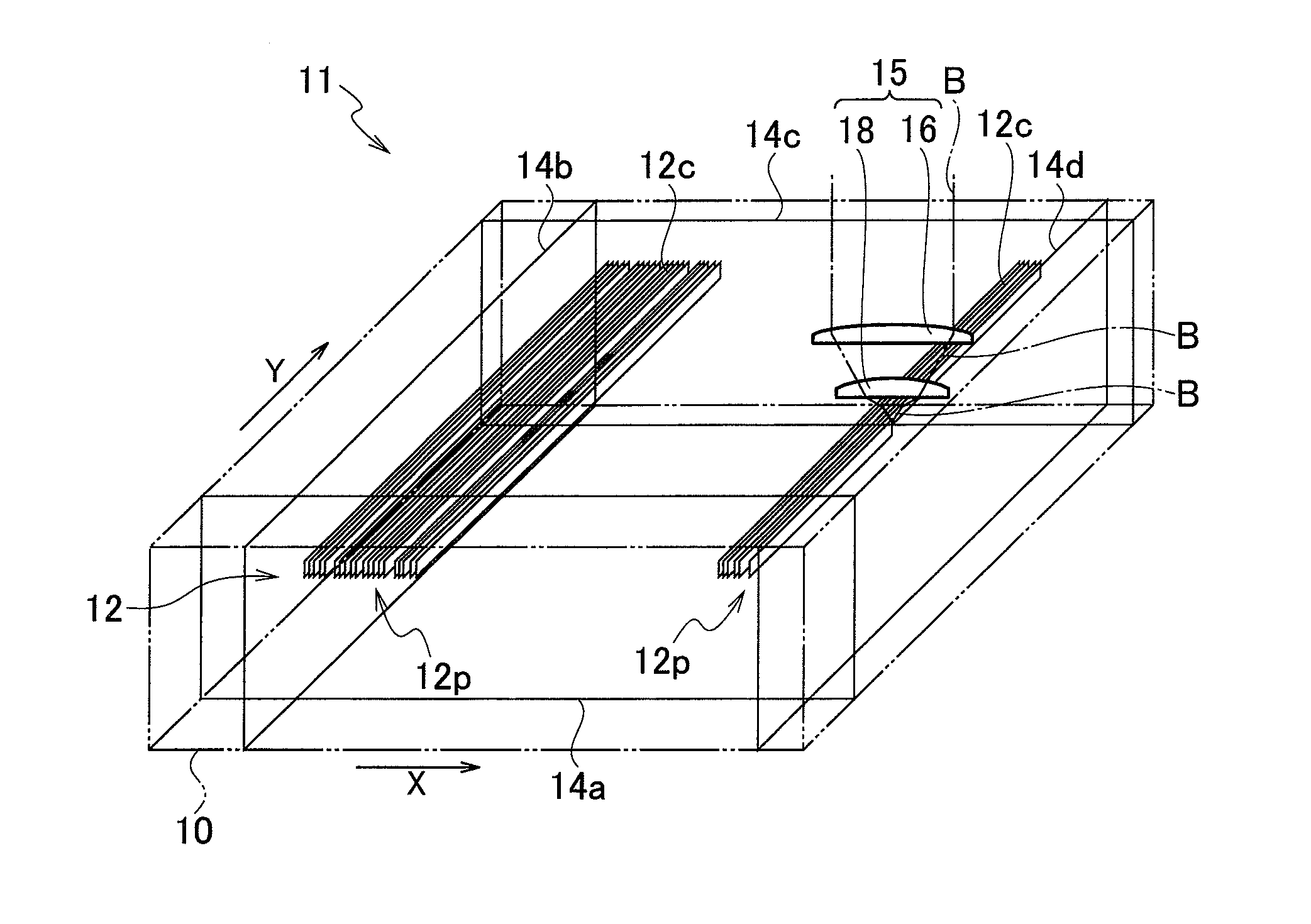
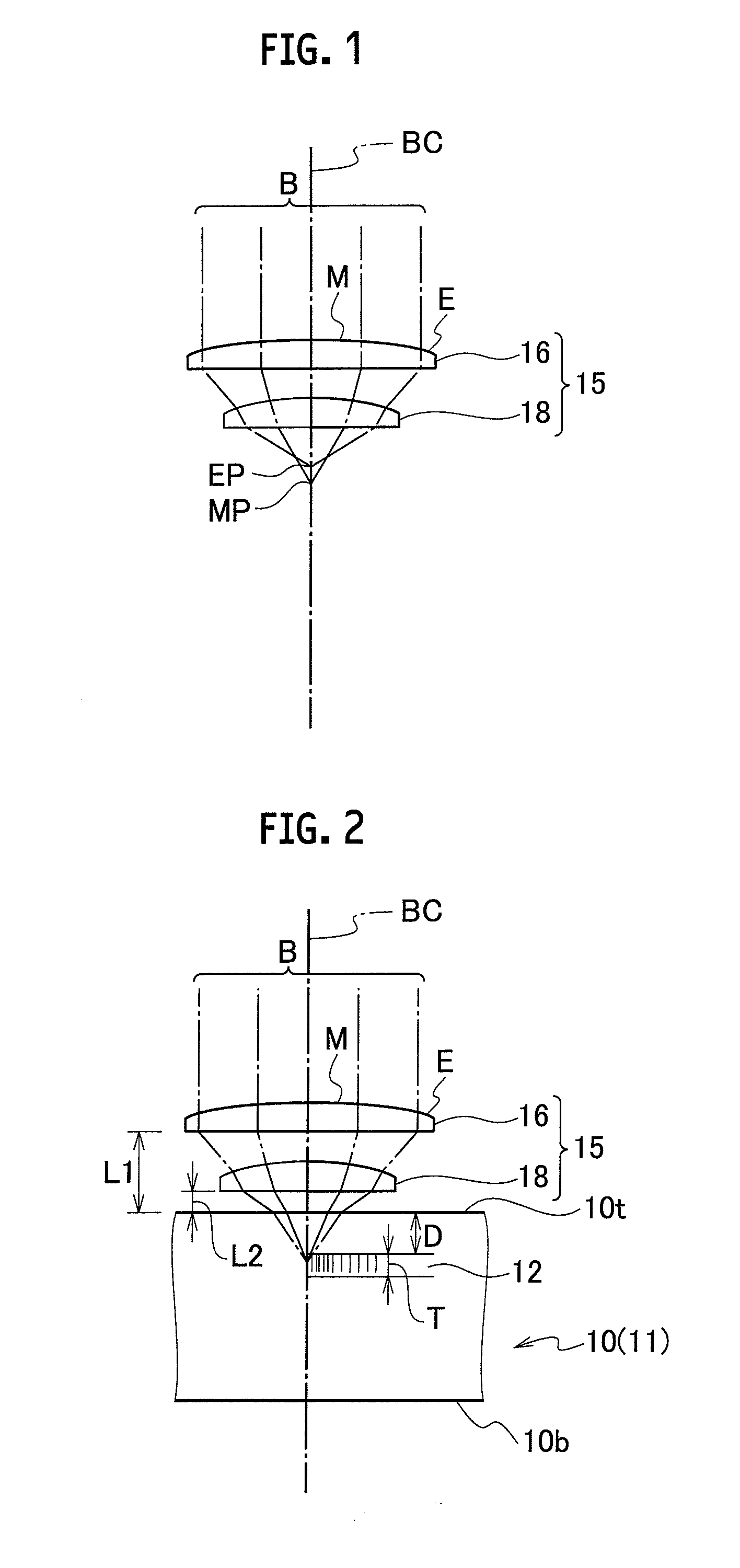
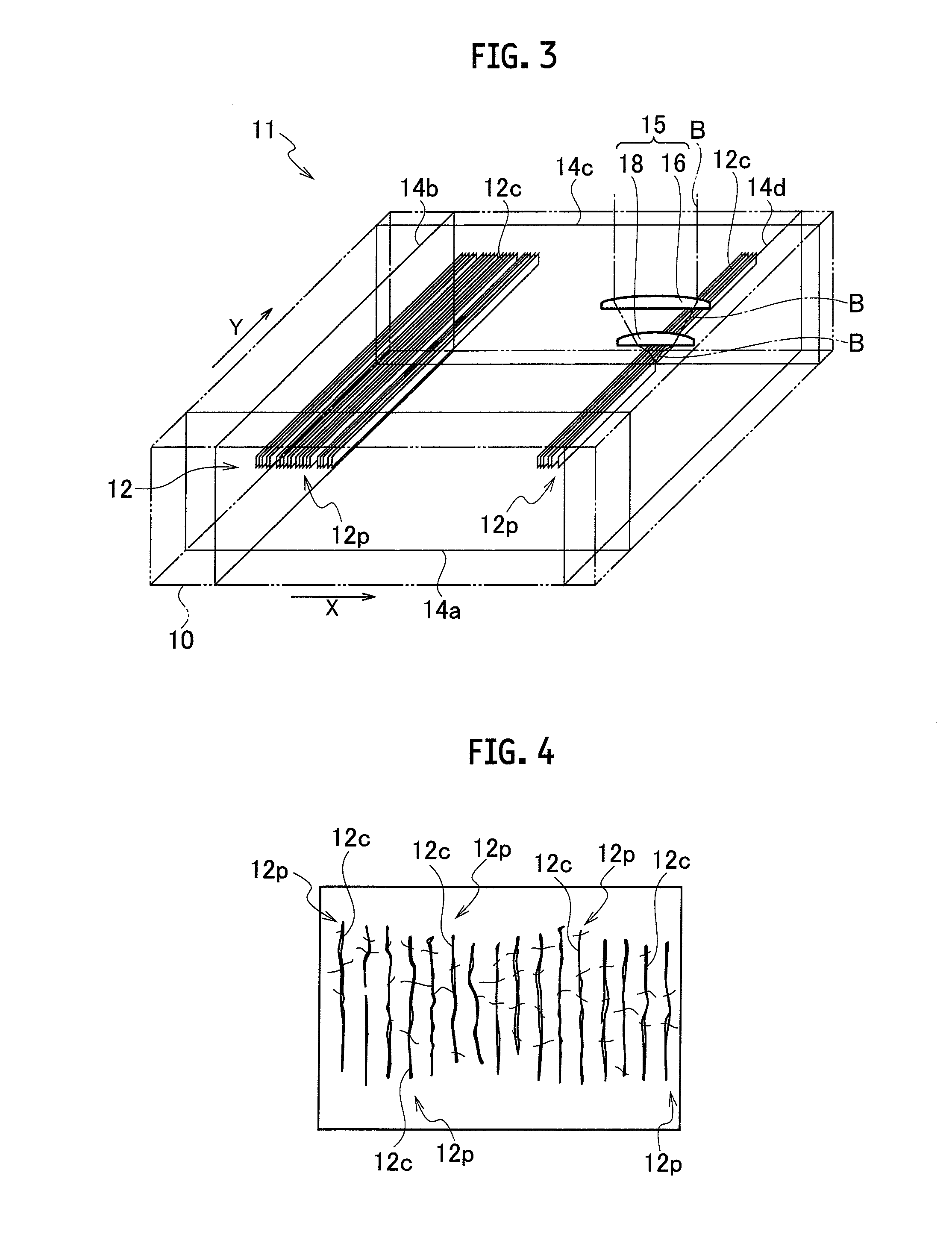
[0040]First, a description is made of a first embodiment. FIG. 1 is a schematic bird's-eye view explaining that laser beams are condensed in air by a laser condenser in this embodiment, and FIG. 2 is a schematic bird's eye view explaining that the laser beams are condensed into an inside of a single crystal member by the laser condenser in this embodiment. FIG. 3 shows a schematic cross-sectional structure explaining a single crystal substrate manufacturing method according to this embodiment and an internal modified layer-forming single crystal member 11 according thereto. FIG. 4 is a schematic cross-sectional view showing that cracks 12c are formed in the inside of the single crystal member by irradiation of the laser beams. FIG. 5 is a schematic perspective cross-sectional view showing that a modified layer 12 formed by the condensation of the laser beams is exposed to a sidewall of the internal modified layer-foaming single crystal member 11.

[0041]The single crystal substrate ma...

second embodiment

[0096]Next, a description is made of a second embodiment. FIG. 17 is a schematic bird's eye view of a single crystal member inside processing apparatus for use in the event of explaining a single crystal substrate manufacturing method according to this embodiment and an internal modified layer-forming single crystal member according thereto.

[0097]A single crystal member inside processing apparatus 69 to be used in this embodiment includes a substrate rotator 74 having: a rotating stage 70 that holds a single crystal member 10 mounted on an upper surface side thereof; and a rotating stage control unit 72 that controls the number of revolutions of the rotating stage 70. Then, the single crystal member inside processing apparatus 69 includes an irradiation device 80 having: a laser light source 76; the condensing lens 15; and a focal point position adjusting tool (not shown) that adjusts a distance from the condensing lens 15 to the rotating stage 70. Moreover, the single crystal membe...


PUM

PropertyMeasurementUnit
Massaaaaaaaaaa
Thicknessaaaaaaaaaa
Distanceaaaaaaaaaa

Abstract

It is an object of the present invention to provide a manufacturing method of a single crystal substrate and to provide an internal modified layer-forming single crystal member, each of which is capable of easily manufacturing a relatively large and thin single crystal substrate. The manufacturing method of a single crystal substrate includes: the step of arranging a condensing lens (15), which emits laser beams (B) and corrects aberration caused by a refractive index of a single crystal member (10), contactlessly on the single crystal member (10); the step of irradiating the laser beams onto a surface (10t) of the single crystal member (10), and condensing the laser beams into an inside of the single crystal member; the step of moving the condensing lens (15) and the single crystal member (10) relatively to each other, and forming a two-dimensional modified layer (12) in the inside of the single crystal member (10); and the step of exfoliating a single crystal layer, which is formed by being divided by the modified layer (12), from the modified layer (12), thereby forming a single crystal substrate.

Description

TECHNICAL FIELD[0001]The present invention relates to a manufacturing method of a single crystal substrate and a manufacturing method of an internal modified layer-forming single crystal member, and particularly, relates to a manufacturing method of a single crystal substrate and a manufacturing method of an internal modified layer-forming single crystal member, each of which cuts out a single crystal substrate thinly and stably.BACKGROUND ART[0002]Heretofore, in the case of manufacturing a semiconductor wafer represented by a single crystal silicon (Si) wafer, such a procedure as below has been adopted. A columnar ingot, which is formed by coagulating silicon melt molten in a quartz crucible, is cut into a block with an appropriate length, a peripheral edge portion thereof is ground so that the ingot cut into the block can have a target diameter, thereafter, the ingot concerned is sliced into a wafer-shaped piece by a wire saw, whereby the semiconductor wafer is manufactured.[0003]...

Claims


Application Information

Patent Timeline
IPC IPC(8): C30B30/00
CPCC30B30/00B28D5/0011H01L21/268C30B33/04C30B33/06C30B29/36H01L21/02532H01L21/02678H01L21/02686H01L21/304B23K26/0665H01L31/18H01L31/1848H01L31/1852H01L31/1892Y02P70/50H01L21/02B23K26/08Y02E10/544
Inventor KUNISHI, YOSUKESUZUKI, HIDEKIMATSUO, RIKAIKENO, JUNICHI
Owner SHIN-ETSU POLYMER CO LTD
Why Eureka
Try Eureka