Compound semiconductor substrate

a technology of compound semiconductor and active layer, applied in the direction of semiconductor devices, basic electric elements, electrical apparatus, etc., can solve the problems of compound semiconductor substrate not being suitable for achieving a normally-off state, low breakdown voltage per unit film thickness, and low efficiency, so as to prevent the cracking of the active layer of nitride from generating, the effect of avoiding warpag

Active Publication Date: 2011-03-17
COORSTEK INC
View PDF1 Cites 62 Cited by
  • Summary
  • Abstract
  • Description
  • Claims
  • Application Information

AI Technical Summary

Benefits of technology

[0021]According to the present invention, it is possible to provide at low cost the compound semiconductor substrate which inhibits the crack of the nitride active layer from generating and avoids the warp caused by thick film formation of the nitride semiconductor.
[0022]Furthermore, th

Problems solved by technology

However, its breakdown voltage per unit film thickness is low and the compound semiconductor substrate suitable for a high breakdown voltage device may not be obtained.
Further, it is not suitable for achieving a no

Method used


Image

  • Compound semiconductor substrate
  • Compound semiconductor substrate
  • Compound semiconductor substrate

Examples


example

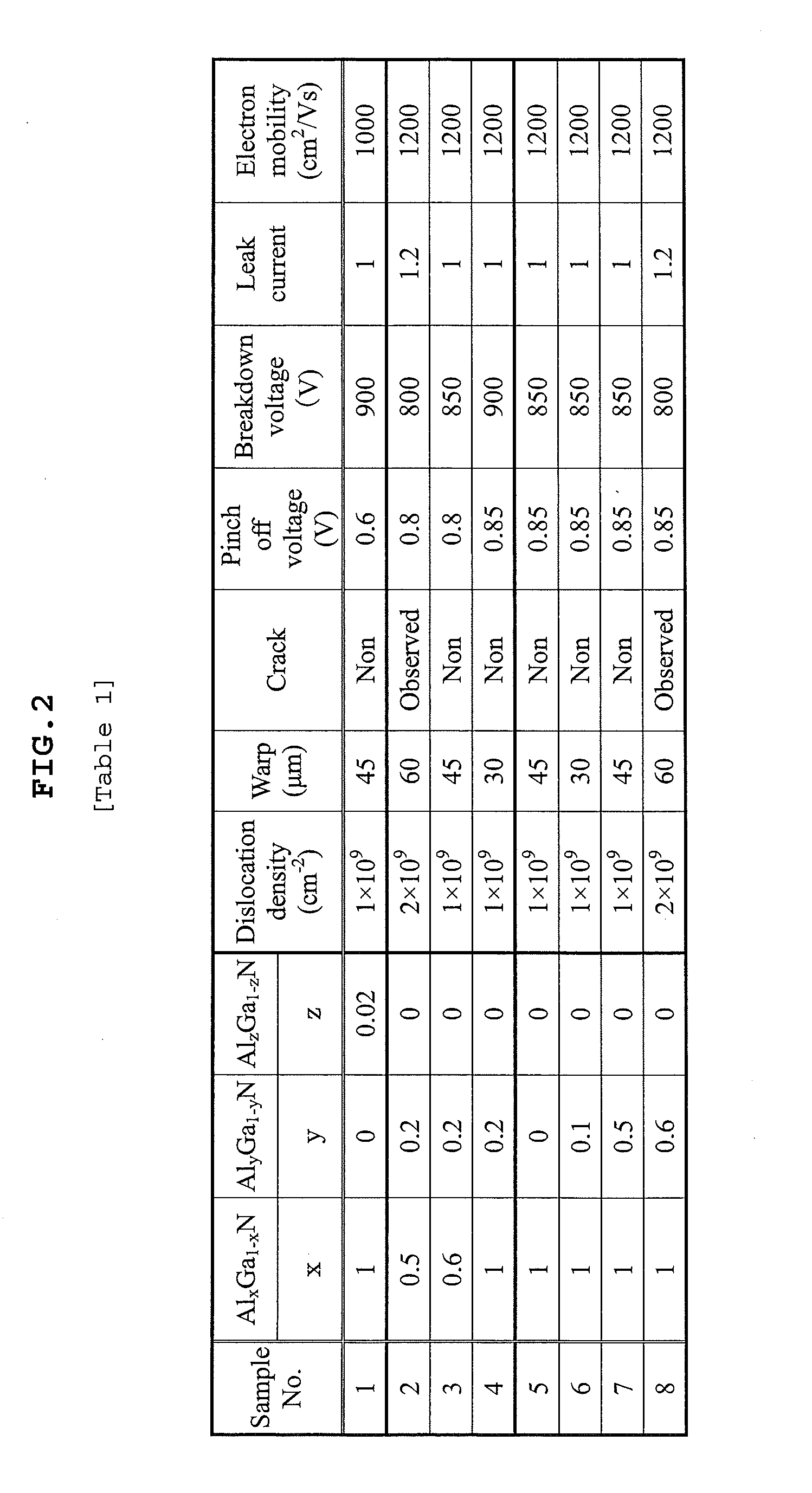
[0082]Hereinafter, the present invention will be described more particularly with reference to Example, but the present invention is not limited to the following Example.

[0083]Samples of a compound semiconductor substrate were produced under the following conditions. Each substrate and a device produced using the substrate were evaluated as follows:

(Evaluation of Substrate)

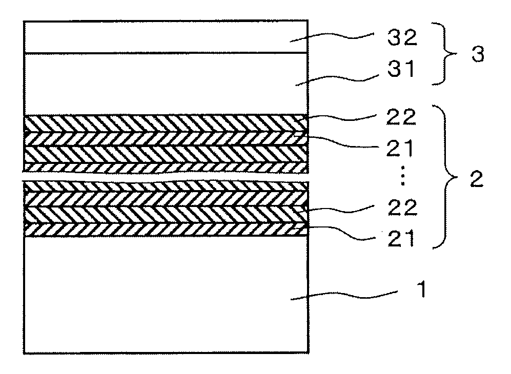
[0084]As for each compound semiconductor substrate sample, a dislocation density in an AlzGa1-zN single crystal layer used as an electron transport layer 31 was evaluated by a transmission electron microscope. Further, the generation of warp and a crack was also evaluated with a laser displacement meter and an optical microscope.

(Evaluation of Device)

[0085]For each compound semiconductor substrate sample, a recess between a recess gate region and an element isolating region was formed by dry etching. A gold (Au) electrode as a gate electrode and aluminum (Al) electrodes as source and drain electrodes were formed o...


PUM


Abstract

A compound semiconductor substrate which inhibits the generation of a crack or a warp and is preferable for a normally-off type high breakdown voltage device, arranged that a multilayer buffer layer 2 in which AlxGa1-xN single crystal layers (0.6≦X≦1.0) 21 containing carbon from 1×10¹⁸ atoms/cm3 to 1×10²¹ atoms/cm3 and AlyGa1-yN single crystal layers (0.1≦y≦0.5) 22 containing carbon from 1×10¹⁷ atoms/cm3 to 1×10²¹ atoms/cm3 are alternately and repeatedly stacked in order, and a nitride active layer 3 provided with an electron transport layer 31 having a carbon concentration of 5×10¹⁷ atoms/cm3 or less and an electron supply layer 32 are deposited on a Si single crystal substrate 1 in order. The carbon concentrations of the AlxGa1-xN single crystal layers 21 and that of the AlyGa1-yN single crystal layers 22 respectively decrease from the substrate 1 side towards the above-mentioned active layer 3 side. In this way, the compound semiconductor substrate is produced.

Description

BACKGROUND OF THE INVENTION[0001]1. Field of the Invention[0002]The present invention relates to a compound semiconductor substrate used preferably for a high speed or high breakdown voltage semiconductor device etc.[0003]2. Description of the Related Art[0004]A semiconductor device using a nitride semiconductor represented by gallium nitride in hexagonal crystal form (GaN), aluminum nitride in hexagonal crystal form (AlN), etc., allows a high breakdown voltage and a high frequency, surpasses properties of a silicon (Si) semiconductor device which is currently dominant, and is expected to be used for power devices etc.[0005]As a method of fabricating the semiconductor device of this type and the compound semiconductor substrate used for its fabrication at low cost, it is known that a buffer area constituted by a plurality of AlGaN-based nitride semiconductor layers whose compositions are different is formed on a silicon (Si) or silicon carbide (SiC) single crystal substrate, and a n...

Claims


Application Information

Patent Timeline
IPC IPC(8): H01L29/20
CPCH01L21/02458H01L21/0254H01L21/02507
Inventor KOMIYAMA, JUNERIGUCHI, KENICHIOISHI, HIROSHIABE, YOSHIHISAYOSHIDA, AKIRASUZUKI, SHUNICHI
Owner COORSTEK INC
Why Eureka
Try Eureka