Semiconductor device and method for manufacturing the same

a technology of semiconductors and components, applied in the direction of semiconductor devices, basic electric elements, electrical apparatus, etc., can solve the problems of housing tilting, affecting reducing the strength of the hanger, so as to improve the accuracy of positioning during mounting, the effect of simple rod shape, and easy insertion and pulling

Active Publication Date: 2007-08-16
NICHIA CORP
View PDF3 Cites 24 Cited by
  • Summary
  • Abstract
  • Description
  • Claims
  • Application Information

AI Technical Summary

Benefits of technology

[0016] With the semiconductor device of the present invention, it is made possible to improve the accuracy of positioning during mounting, too, by taking advantage of the grooves formed in the side surfaces of the housing so as to penetrate therethrough. When a guide bar which fits in the groove is provided on the suction nozzle of the chip mounter which transfers the semiconductor device, for example, displacement of the semiconductor device caused by breaking the vacuum after the transfer of the semiconductor device can be suppressed. A guide pin which fits into the groove may also be provided on the circuit board whereon the device is to be mounted. Since the groove penetrates from the top through the bottom, the guide bar or the guide pin can be easily inserted and pulled out either from the top or the bottom. The guide bar and the guide pin may have simple rod shape. In case the light emitting device is used in combination with an optical component such as optical guide, for example, the light emitting device and the optical component can be easily positioned by providing a positioning member at a predetermined position of the optical component which fits into the groove of the light emitting device.
[0017] With the semiconductor device described above, in case the groove has a width substantially equal to the thickness of the lead electrode, there may a case of supporting the housing by fitting a part of the lead frame into the groove. Since the groove penetrates from the top through the bottom, the housing can be engaged with the circumference of the opening formed in the lead frame which has higher strength, not on a hanger lead of thin band shape as in the prior art. This en...

Problems solved by technology

However, decreasing the thickness of the light emitting device having the constitution disclosed in Japanese Unexamined Patent Publication (Kokai) No. 2004-363537 gives rise to some problems.
For example, when a low-profile light emitting device is manufactured by using lead frame provided with hanger lead, it is necessary to decrease the width of the hanger lead which results in a decrease in strength of the hanger lead.
This increases the possibility of such troubles to occur as the hanger lead is subjected to torsional deformation when the lead frame provided with hanger lead is transported, thus causing the ho...

Method used


Image

  • Semiconductor device and method for manufacturing the same
  • Semiconductor device and method for manufacturing the same
  • Semiconductor device and method for manufacturing the same

Examples


Embodiment Construction

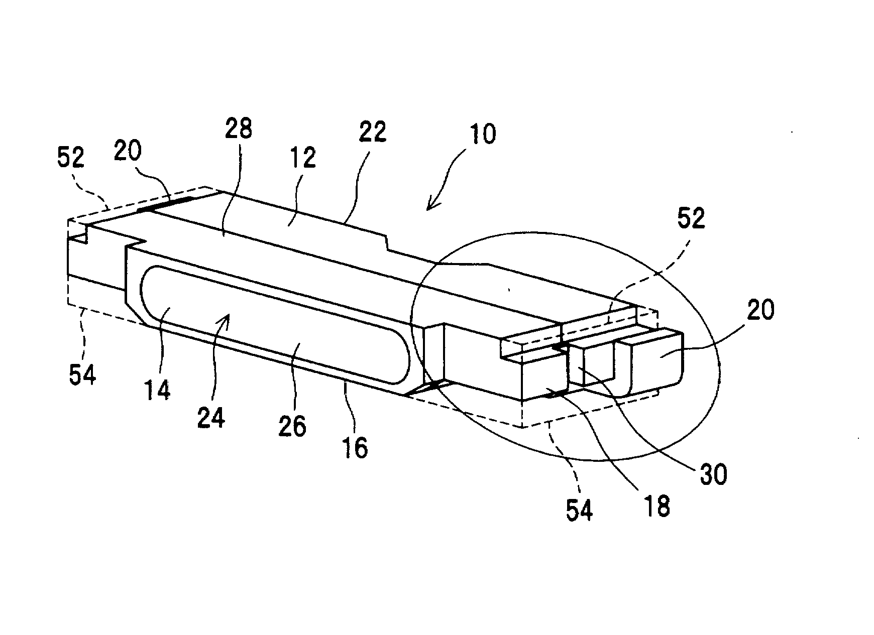
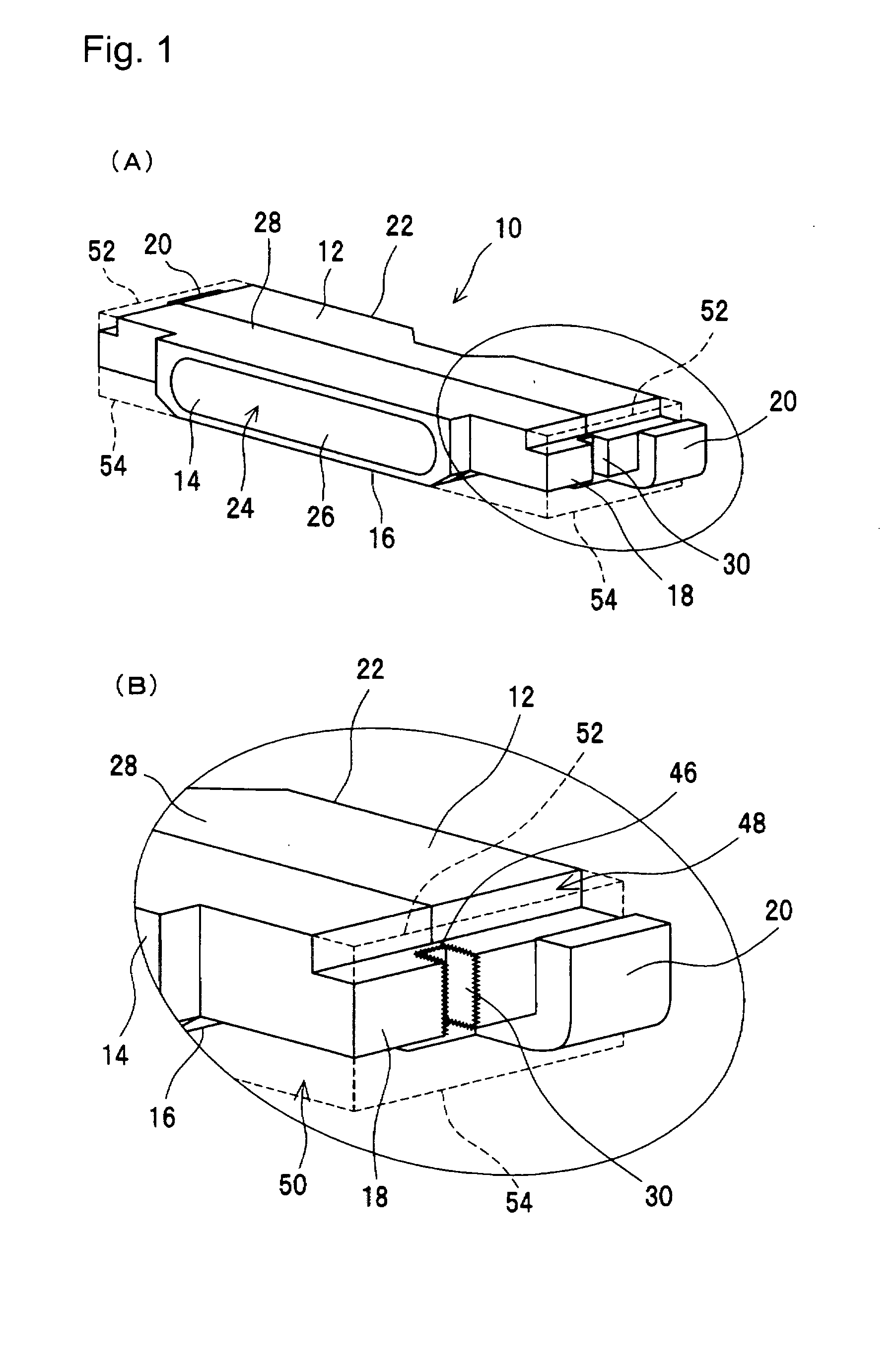
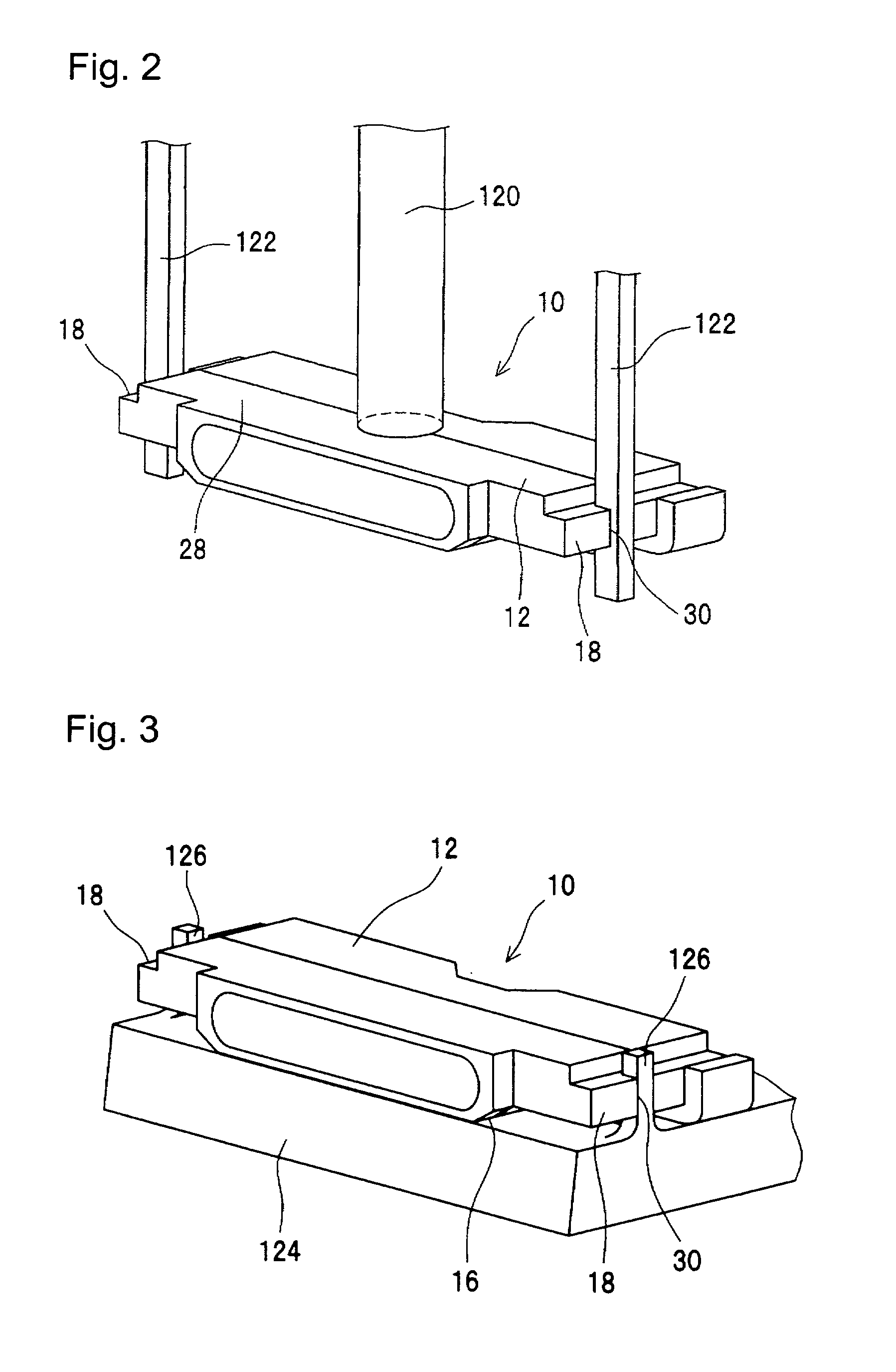
[0050] The light emitting device 10 shown in FIG. 1 comprises a housing 12 of flat shape and a lead electrode 20 which is bent from a bottom surface 16 along a side surface 18 of the housing 12. Front surface of the housing 12 serves as a light emitting surface 14, with a recess 24 formed so as to open in the light emitting surface 14 and extends toward the back surface 22. The opening of the recess 24 constitutes a window for light emission. The recess 24 is filled with a translucent resin 26 so as to seal a semiconductor light emitting element (not shown) which is mounted in the recess 24. A groove 30 is formed in the side surface 18 of the housing 12 to extend in parallel to the light emitting surface 14. The groove 30 penetrates from the top surface 28 through the bottom surface 16 of the housing 12. The housing 12 serves as a support member which supports a semiconductor 1, light emitting device and the distal end of the lead electrode 20, and also as a protective member which ...


PUM


Abstract

The present invention provides a semiconductor device having a structure which is suitable for reduction in thickness and weight.
The semiconductor device 1 comprises a housing 12 which has the recess 24 in the front surface 14, the pair of lead electrodes 20 which have the distal ends 34 exposed in the recess 24, protrude from the external surface of the housing 12 and are bent along the bottom surface 16 of the housing 12, and a semiconductor element 36 which is housed in the recess 24 and is electrically connected to the pair of lead electrodes 20. The housing 12 has the grooves 30 which are formed on the pair of side surfaces 18 which adjoin the front surface 14 and the bottom surface 16 on the right and left sides so as to penetrate the housing 12 from the top surface 28 toward the bottom surface 16 of the housing 12. The grooves 30 preferably have width substantially equal to the thickness of the lead electrode 20. The grooves 30 are more preferably formed to be flush with the distal ends 34 of the lead electrode 20.

Description

BACKGROUND OF THE INVENTION [0001] 1. Field of the Invention [0002] The present invention relates a light emitting device using a semiconductor light emitting element, and a light receiving device used in an optical sensor or the like, and, more particularly, to a low-profile light emitting device used as the backlight of a liquid crystal display. [0003] 2. Description of the Related Art [0004] In recent years, the backlight of a liquid crystal display employs a surface-emitting light source comprising a low-profile light emitting device and an optical guide which spreads the light emitted by the light emitting device. One among the light emitting devices used in such applications is a low-profile light emitting device comprising a light emitting diode disposed in a flat housing made of a resin (refer to, for example, Japanese Unexamined Patent Publication (Kokai) No. 2004-363537). The resin housing has such a constitution as a protrusion is provided on an elongated light emitting s...

Claims


Application Information

Patent Timeline
IPC IPC(8): H01L33/00H01L33/56H01L33/62
CPCY10S438/973H01L33/483H01L24/97H01L2224/45124H01L2224/45144H01L2224/45147H01L2224/45169H01L2224/48247H01L2224/48257H01L2924/01322H01L2924/12041H01L2924/00H01L2924/00014
Inventor YAMAMOTO, SAIKI
Owner NICHIA CORP
Why Eureka
Try Eureka