
Light emitting device and method of fabricating the same

Active Publication Date: 2007-08-16
SHIN-ETSU HANDOTAI CO LTD
View PDF2 Cites 16 Cited by
  • Summary
  • Abstract
  • Description
  • Claims
  • Application Information

AI Technical Summary

Benefits of technology

[0007] It is therefore an object of the this invention to provide a light emitting device allowing effective use of the GaAs single crystal substrate assisting thereon growth of the light emitting layer portion, having completely been removed in the conventional process, as a constituent of the functional device, and also capable of raising the extraction efficiency of beam to the external, and to provide a method of fabricating the same.

Problems solved by technology

Efficiency of extracting light from the device is, therefore, a critical issue for every effort of obtaining the device of further higher luminance.
The AlGaInP alloy composing the light emitting layer portion, however, has a band gap larger than that of GaAs, and is therefore disadvantageous in that the emitted light is absorbed by the device substrate portion, so that a sufficient level of light extraction efficiency is hard to obtain.
It should, however, be said too wasteful indeed to completely remove the GaAs substrate, which is considerably more expensive as compared with silicon substrates, without paying no attention about use thereof and to separately provide the reinforcing silicon substrate, yet the top priority is placed on light extraction efficiency.
The GaAs substrate assisting growth of the light emitting layer portion also plays a role of providing necessary strength against handling in the device fabrication, so that it is obvious that, if the GaAs substrate is removed, only the very thin light emitting layer portion will never ensure necessary strength against handling or the like.

Method used


Image

  • Light emitting device and method of fabricating the same
  • Light emitting device and method of fabricating the same
  • Light emitting device and method of fabricating the same

Examples


first embodiment

[0117] A mode of carrying out the first embodiment of this invention will be described below referring to the attached drawings.

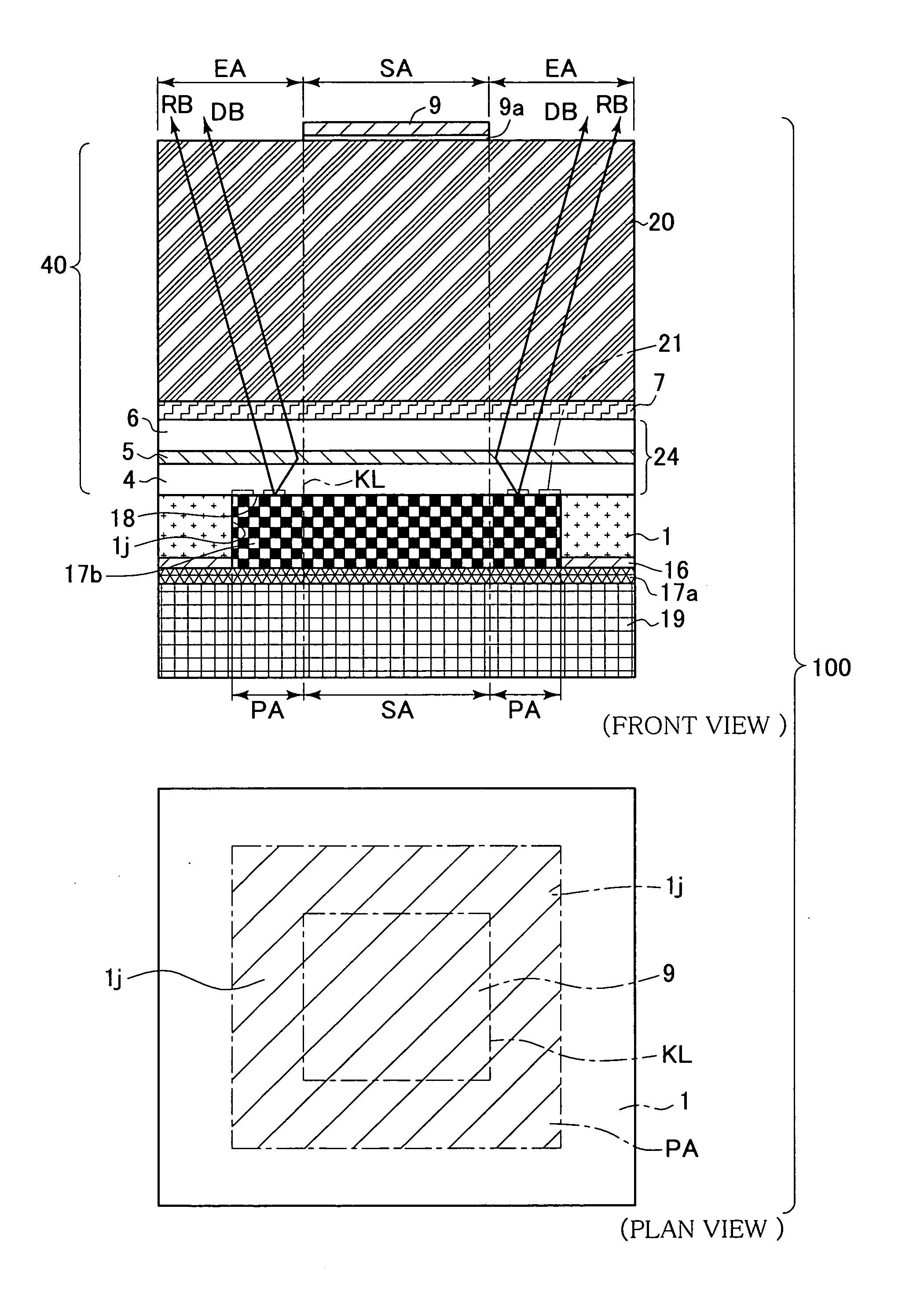
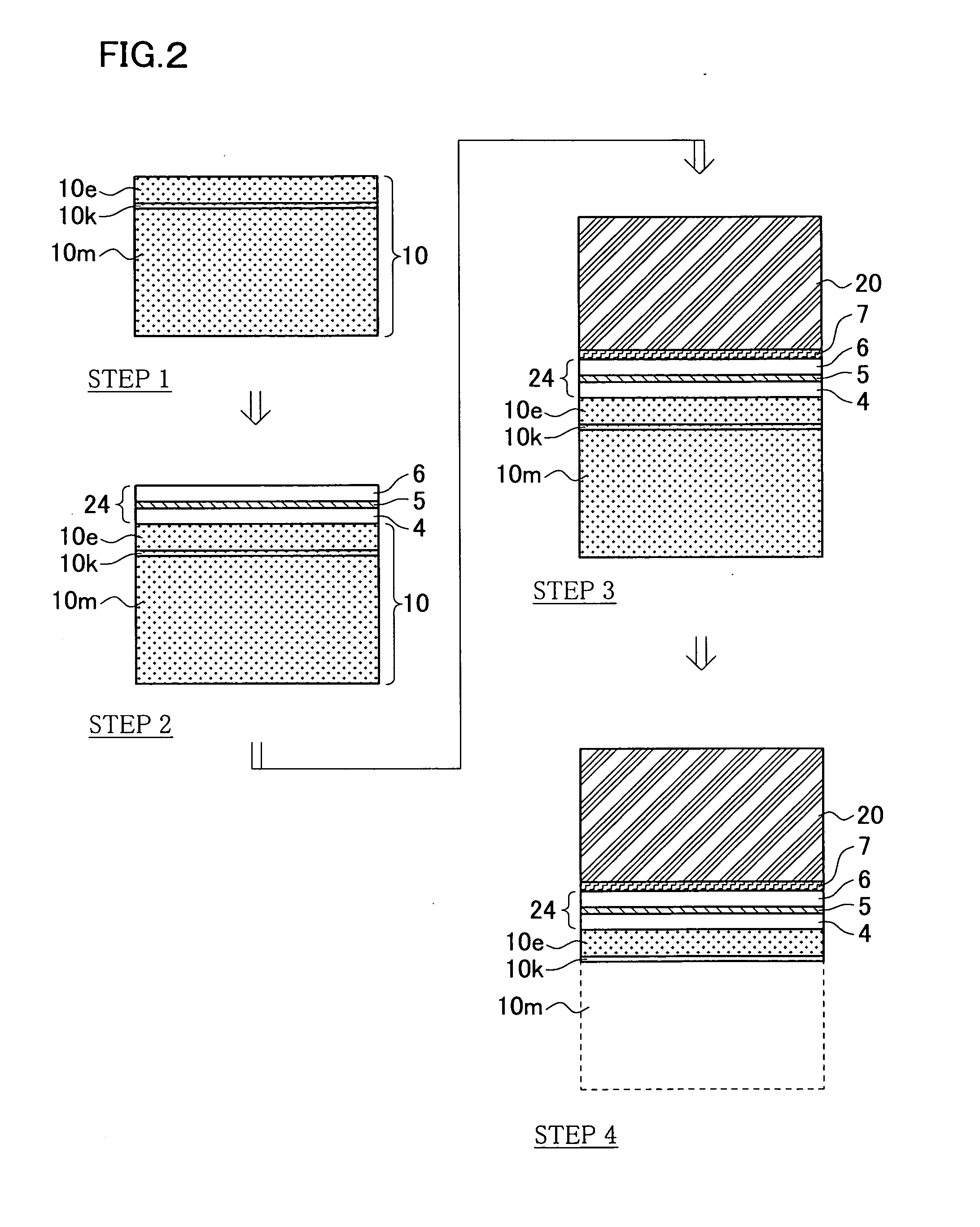
[0118]FIG. 1 is a schematic drawing of a light emitting device 100 as one example of the first embodiment. The light emitting device 100 has a main compound semiconductor layer 40 having therein a light emitting layer portion 24, formed on a first main surface of a residual substrate portion 1. A main light extraction surface EA is formed on the first main surface side of the main compound semiconductor layer 40, and a light-extraction-side electrode 9, through which emission drive voltage is applied to a light emitting layer portion 24, is formed so as to cover a part of the first main surface of the main compound semiconductor layer 40. An opening 1j, as the cut-off portion opened on the second main surface of the residual substrate portion 1, is formed by partially cutting off the residual substrate portion 1, wherein a part of the residual substrate po...

second embodiment

(Mode A)

[0136]FIG. 11 schematically shows a light emitting device 1100 as an example of the second embodiment of this invention. There are many aspects common to those in the light emitting device 100 shown in FIG. 1, so that paragraphs below will explain only differences reside therein. That is, the aspects other than those described below are configured similarly to as in the light emitting device 100 shown in FIG. 1, so that the explanation of the first embodiment will be applied herein, rather than repeating the detailed explanations. Common elements are given with common reference numerals. The light emitting device 1100 has the main compound semiconductor layer 40, having therein the light emitting layer portion 24, epitaxially grown on the first main surface of the sub-substrate 10e (see FIG. 12). The main light extraction surface EA is formed on the first main surface side of the main compound semiconductor layer 40, and the light-extraction-side electrode 9, through which...

third embodiment

[0161] Paragraphs below will explain the third embodiment of this invention, referring to the attached drawings. FIG. 26 schematically shows a light emitting device 2100 as an example of the third embodiment of this invention. There are many aspects common to those in the light emitting device 100 shown in FIG. 1, so that paragraphs below will explain only differences reside therein. That is, the aspects other than those described below are configured similarly to as in the light emitting device 100 shown in FIG. 1, so that the explanation of the first embodiment will be applied herein, rather than repeating the detailed explanations. Common elements are given with common reference numerals.

[0162]FIG. 26 schematically shows the light emitting device 2100 as an example of the third embodiment of this invention. In light emitting device 2100, the main compound semiconductor layer 40 having therein the light emitting layer portion 24 is epitaxially grown on the first main surface of t...


PUM


Abstract

A composite growth-assisting substrate 10 is formed by epitaxially growing a separation-assisting compound semiconductor layer 10k composed of a non-GaAs III-V compound semiconductor single crystal, and then a sub-substrate 10e composed of a GaAs single crystal in this order, on a first main surface of a substrate bulk 10m composed of a GaAs single crystal. The sub-substrate portion 10e is then separated from the composite growth-assisting substrate 10, so as to be left as a residual substrate portion 1 on a second main surface of the main compound semiconductor layer 40, and a portion of the residual substrate portion 1 is cut off to thereby form a cut-off portion 1j having a bottom surface used as a light extraction surface. By this configuration, the light emitting device is provided as allowing effective use of the GaAs substrate, and increasing the light extraction efficiency.

Description

BACKGROUND OF THE INVENTION [0001] 1. Field of the Invention [0002] This invention relates to a light emitting device and a method of fabricating the same. [0003] 2. Description of the Related Art [0004] After years of advancement, materials and element structures applied to light emitting elements such as light emitting diode and semiconductor laser devices have become more and more closer to the theoretical limits in terms of photo-electric conversion efficiency inside the device. Efficiency of extracting light from the device is, therefore, a critical issue for every effort of obtaining the device of further higher luminance. For example, a light emitting device having the light emitting layer portion thereof composed of an AlGaInP alloy can be realized as a high-luminance device, by adopting a double heterostructure in which a thin AlGaInP (or GaInP) active layer is sandwiched between an n-type AlGaInP cladding layer and a p-type AlGaInP cladding layer, both having larger band g...

Claims


Application Information

Patent Timeline
IPC IPC(8): H01L33/00H01L33/10H01L33/30H01L33/40H01L33/62H01S5/323
CPCH01L33/405H01L33/0079H01L24/32H01L2224/32245H01L2224/48091H01L2224/48137H01L2224/48247H01L2224/48463H01L2224/49107H01L2224/73265H01L2224/92247Y10S438/977Y10S438/97H01L2224/45144H01L33/0093H01L2924/00014H01L2924/00
Inventor YAMADA, MASATOTAKAHASHI, MASANOBU
Owner SHIN-ETSU HANDOTAI CO LTD
Features
  • Generate Ideas
  • Intellectual Property
  • Life Sciences
  • Materials
  • Tech Scout
  • Unparalleled Data Quality
  • Higher Quality Content
  • 60% Fewer Hallucinations
Learn More