Electronic assembly with detachable components

a technology of electronic components and components, applied in the direction of non-printed jumper connection addition, circuit inspection/indentification, test/measurement of semiconductor/solid-state devices, etc., can solve the problems of difficult removal of soldered or wire-bonded components for repair or reuse, and the cost of sockets is rather high, so as to facilitate the placement of components, eliminate the insertion step of acm, and the effect of easy removal

Inactive Publication Date: 2007-08-16
WINTEC IND INC
View PDF60 Cites 50 Cited by
  • Summary
  • Abstract
  • Description
  • Claims
  • Application Information

AI Technical Summary

Benefits of technology

[0008]An alignment chain can monitor the positional and contact integrity for a group of components on a substrate in an electronic assembly. By incorporating conductive pads as alignment marks at predetermined regions in a component and incorporating conductive pads as reference marks at designated regions on the substrate to match the positions of alignment marks at the component to be placed on the substrate, an alignment chain can be built. The alignment chain is formed by linking the alignment marks at a group of components with the matching reference marks on the substrate over an ACM interconnect layer from component to component to create a serial, continuous conduction path among the group of components to be monitored. Depending upon the complexity of the electronic assembly, the alignment chain may be divided into multiple smaller alignment chains to detect the positional and contact integrity for a smaller group of components linked in a chain by monitoring its conduction status. The technique allows components to be detached for reuse.
[0009]In different embodiments of the invention, an electronic assembly may stack multiple substrates into a more compact three-dimensional structure. Interconnection elements can be used to facilitate the interconnection between neighboring substrates in a stacked assembly. The interconnection element comprises a pre-fabricated conductive path or routing trace in a planar structure or package for insertion into a fixture opening or an embossed cavity on the substrate to interconnect neighboring substrates across ACM layers. The interconnection elements can replace expensive socket, mechanical connector, or flexible ribbon circuit with minimal positional constraint on the substrate to simplify the design of an electronic assembly.
[0011]Some exemplary methods of using anisotropic conductive material in an electronic assembly are illustrated. One exemplary method uses a substrate comprising embossed cavities to facilitate the placement of components and an anisotropic conducting membrane at the embossed cavity as a component interconnect layer to the substrate. The ACM may be directly laminated at the component interconnect surface to eliminate the ACM insertion step in manufacturing the electronic assembly. An alternative exemplary method is the use of an aligning fixture in the electronic assembly. The aligning fixture can be aligned to a substrate by using a placement equipment and bonded to the substrate by using anisotropic conductive paste or solder paste, if the fixture also contains an interconnect circuitry. Alternatively, a sheet of ACM may be placed on the substrate surface prior to the placement of the fixture. Both the embossed cavities on the substrate and the openings at the fixture can hold components on the target land patterns at the substrate with accuracy. Alignment marks or alignment mechanism may be incorporated in the fixture to align with matching reference marks or reference mechanisms at the substrate, although an optical pattern recognition technique may be used to align fixture to substrate.
[0012]Benefits of exemplary implementations of the invention include the use of the ACM layer to replace solder paste or wire-bonding in a conventional component assembly. By using ACM as a component interconnect layer and using a fixture or embossed cavity at the substrate, components can be readily removed and reattached to an electronic assembly. Components that are expensive or in short supply can be readily detached and reused in different electronic assemblies. Defective components may be easily removed at rework. Furthermore, components can be detached and replaced in a system upgrade. This flexibility results because the ACM layer allows components to be readily detached and reattached in an electronic assembly without necessitating desoldering or cutting wire-bond that may damage the component or other parts of the assembly.

Problems solved by technology

One problem with both the SMT and the COB technique is that a soldered or wire-bonded component is typically difficult to remove for repair or reuse once it is attached to the substrate.
The sockets are rather expensive.

Method used


Image

  • Electronic assembly with detachable components
  • Electronic assembly with detachable components
  • Electronic assembly with detachable components

Examples


Embodiment Construction

[0023]Detailed descriptions of exemplary embodiments are provided herein. It is to be understood, however, that the present invention may be embodied in various forms. Therefore, specific details disclosed herein are not to be interpreted as limiting, but rather as a basis for the claims and as a representative basis for teaching one skilled in the art to employ embodiments of the present invention in virtually any appropriately detailed system, structure, or manner.

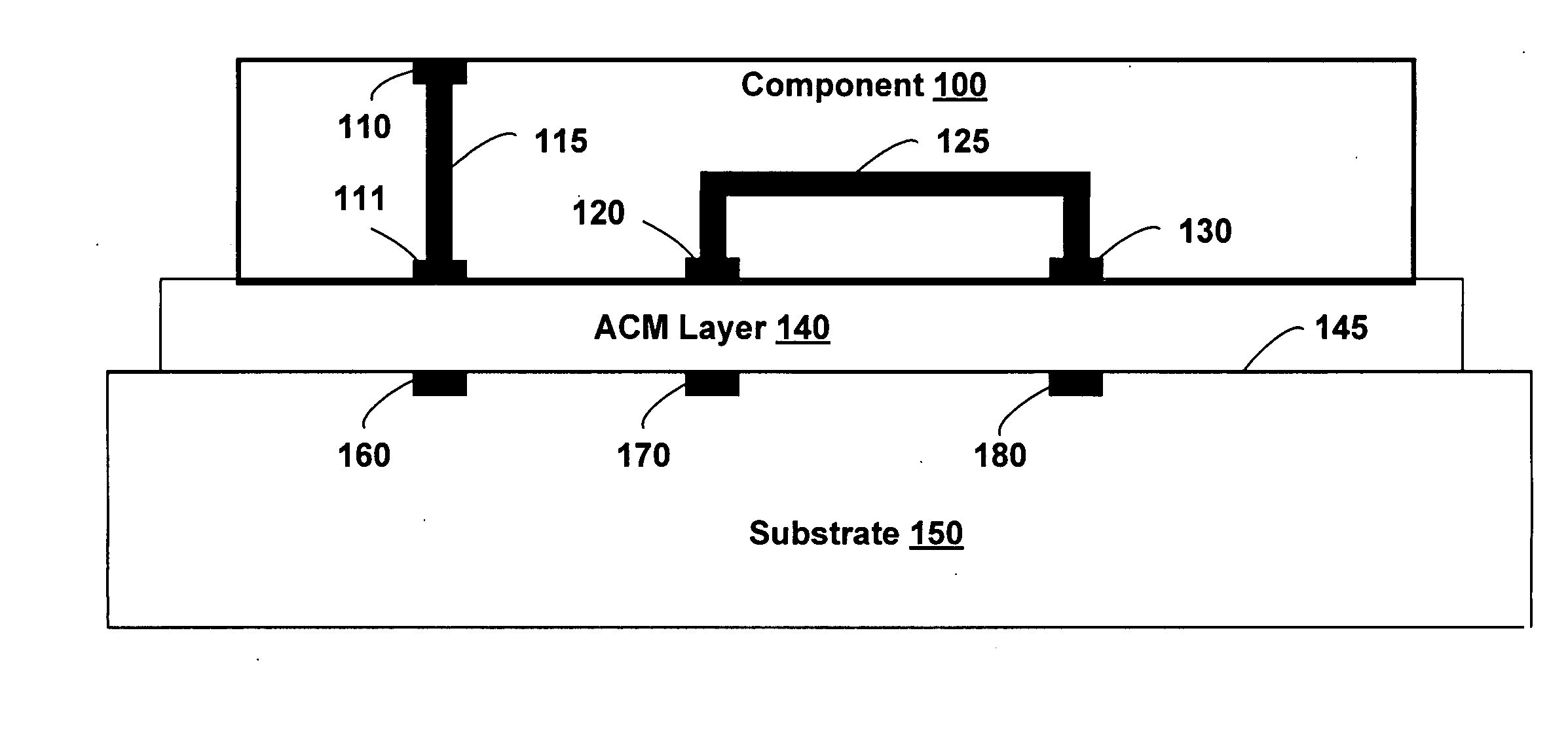
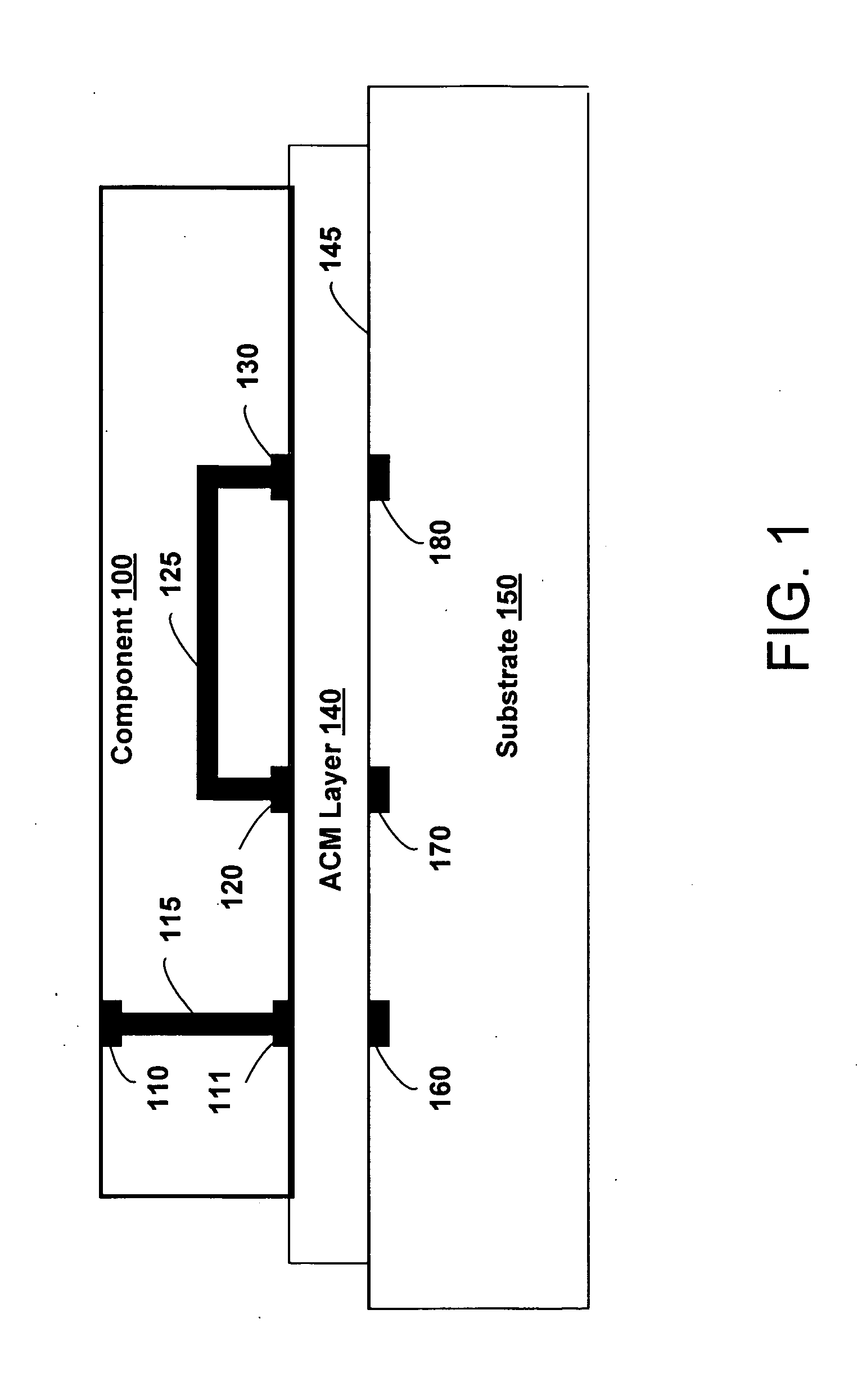
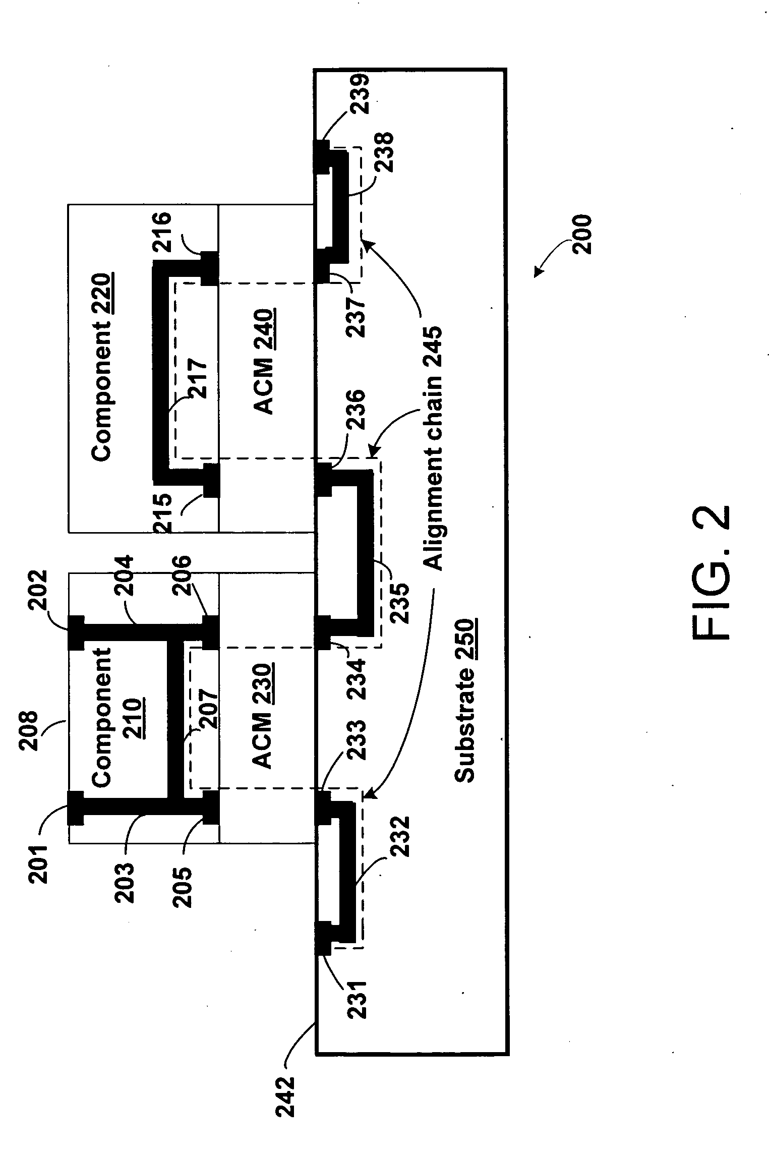
[0024]An exemplary embodiment is an electronic assembly comprising detachable components assembled on a substrate via an anisotropic conductive material as an interconnect layer. The electronic assembly may comprise alignment chains to monitor positional and contact integrity of components on the substrate across the interconnect layer comprising the anisotropic conductive material.

[0025]Electronic assemblies, such as flash cards, add-on boards, or memory modules, have components soldered or wire-bonded on substrate, whi...


PUM

PropertyMeasurementUnit
electricallyaaaaaaaaaa
conductiveaaaaaaaaaa
thermal dissipationaaaaaaaaaa

Abstract

The present invention provides systems and methods for assembling an electronic assembly using an anisotropic conducting membrane (ACM) as a component interconnect and a substrate embossed with placement cavities or a positional fixture to facilitate component placement on the substrate in the electronic assembly. The fixture may comprise multiple layers of interconnects to improve routing density for the electronic assembly enclosed in a housing. An alignment chain may be used to monitor positional and contact integrity of the ACM interfaced components in a complex assembly. The systems and methods allow components to be detached for reuse. Interconnection elements or conduction pathways at the components can be used to interconnect a plurality of neighboring substrates over the ACM layers into a stacked electronic assembly.

Description

CROSS-REFERENCE TO RELATED APPLICATIONS[0001]This application is a continuation-in-part of U.S. patent application Ser. No. 11 / 351,418 entitled “Apparatus and Method for Predetermined Component Placement to a Target Platform,” filed Feb. 10, 2006, which is hereby incorporated by reference.BACKGROUND[0002]1. Field of the Invention[0003]The present invention relates generally to electronic assemblies, and more particularly to assembly techniques on the use of anisotropic conducting material as a component interconnect and the use of substrate embossed with placement cavities or the use of positional fixtures to facilitate the placement of component on the substrate in an electronic assembly.[0004]2. Related Art[0005]Electronic assemblies are typically assembled by using surface mount technology (SMT), or more recently, the chip-on-board (COB) technology. Using SMT, packaged electronic components are soldered on a substrate, such as a printed circuit board (PCB), by printing a thin lay...

Claims


Application Information

Patent Timeline
Patent Type & Authority Applications(United States)
IPC IPC(8): H01L23/29
CPCH01L23/041Y10T29/49133H01L23/4093H01L23/481H01L23/544H01L24/29H01L24/32H01L24/33H01L24/72H01L25/0655H01L2223/54426H01L2223/5446H01L2223/54466H01L2223/54473H01L2924/01078H01L2924/01079H01L2924/14H01L2924/15192H01L2924/19041H01L2924/19042H01L2924/19043H05K1/0268H05K1/144H05K3/222H05K3/325H05K2201/0314H05K2201/10159H05K2201/10378H05K2203/167H01L2224/29H01L2924/01033H01L2924/014H01L2224/29101H01L23/10Y10T29/49004H05K7/20436H05K3/303H05K1/16H05K1/0296H01L2924/00013H01L2224/29444H01L2224/2929H01L2224/2939H01L2924/0105H01L2924/01006H01L2924/00014H01L2924/00H01L2224/29099H01L2224/29199H01L2224/29299H01L23/29H01L22/34H01L21/67259H01L22/32
Inventor CHEN, KONG-CHEN
Owner WINTEC IND INC
Why Eureka
Try Eureka