Exhaust buildup monitoring in semiconductor processing

a technology of exhaust buildup and semiconductor processing, which is applied in the direction of heat measurement, instruments, coatings, etc., can solve the problems of ruinous process equipment contamination, difficult scheduling, and contamination entering other adjacent processing systems, and achieves simple and passive operation and data collection, and avoids invasive monitoring procedures. , the effect of reducing the cost of material and maintenan

Inactive Publication Date: 2007-08-16
TOKYO ELECTRON LTD
View PDF8 Cites 7 Cited by
  • Summary
  • Abstract
  • Description
  • Claims
  • Application Information

AI Technical Summary

Benefits of technology

[0010] The invention provides a monitoring function that is inexpensive in both material and maintenance. Simple and passive operation and data collection are provided. Invasive monitoring procedures are avoided while invasive cleaning and build up failure are minimized.

Problems solved by technology

Some of these particles can move upstream during the cycling of the system or can contaminate the environment around the processing equipment that can lead to contamination entering other adjacent processing systems.
A problem with the scheduling of exhaust line cleaning is to insure that the line is cleaned before a structural failure of the deposits within it that could cause a ruinous contamination of the process equipment.
This scheduling is made difficult by the unpredictable growth rate of the deposit buildup.
Conservative scheduling of the cleaning of the lines to insure that the cleaning is not deferred too long results in unnecessary downtime of the equipment and unnecessary increase of the cleaning costs.
However, the inspection itself reduces the productivity of the equipment, and the invasive monitoring itself can lead to the unnecessary production of particles.

Method used


Image

  • Exhaust buildup monitoring in semiconductor processing
  • Exhaust buildup monitoring in semiconductor processing
  • Exhaust buildup monitoring in semiconductor processing

Examples


Embodiment Construction

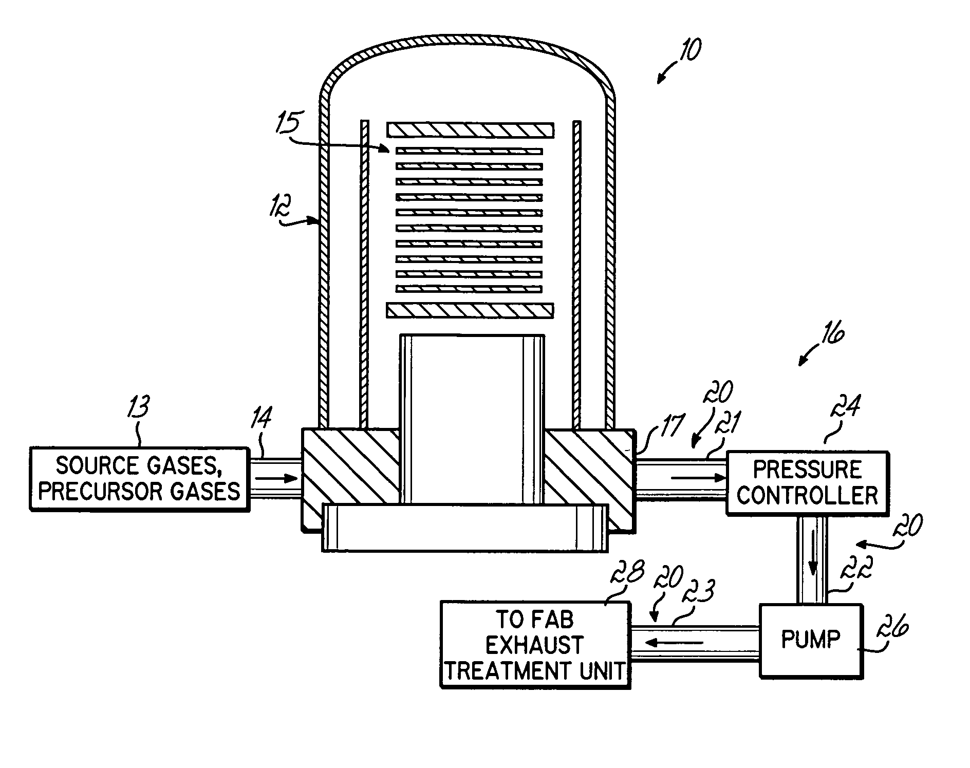
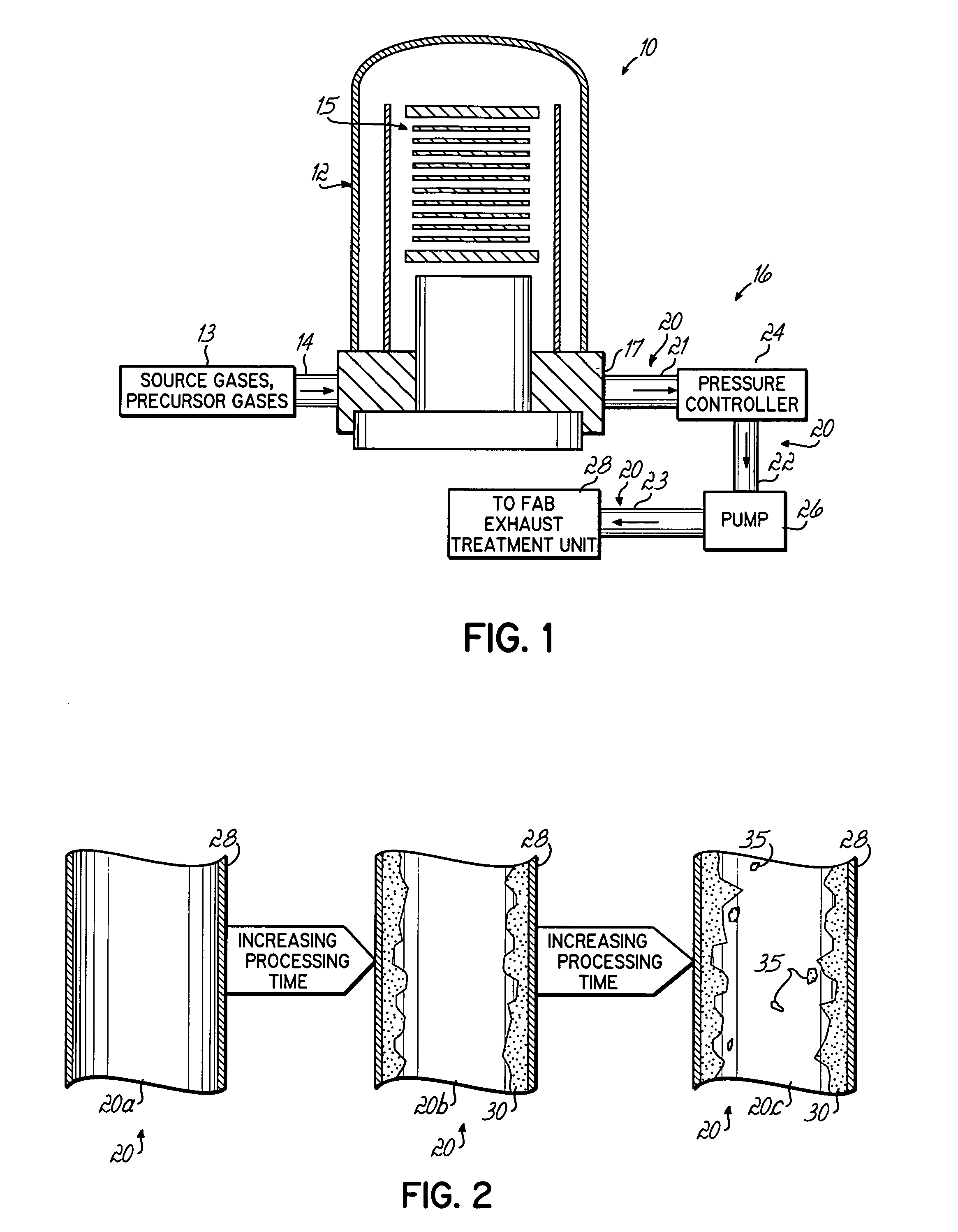
[0017] The diagram of FIG. 1 illustrates a semiconductor wafer processing system 10 which is, in the illustration, a batch chemical vapor deposition system having a gas supply system 13 connected to an inlet 14 of a vacuum processing chamber 12 in which are processed semiconductor wafers 15, and an outlet system 16 for removing spent gases from the chamber 12 connected to an outlet 17 of the chamber 12. While illustrated as a batch CVD system, the processing system 10 can be any type of semiconductor processing system that has a tendency to accumulate a buildup of deposits in exhaust lines of the outlet system 16. Such systems might include deposition and etching systems, thermal or other processing systems, physical, chemical systems or other processing systems having the problem solved by the invention.

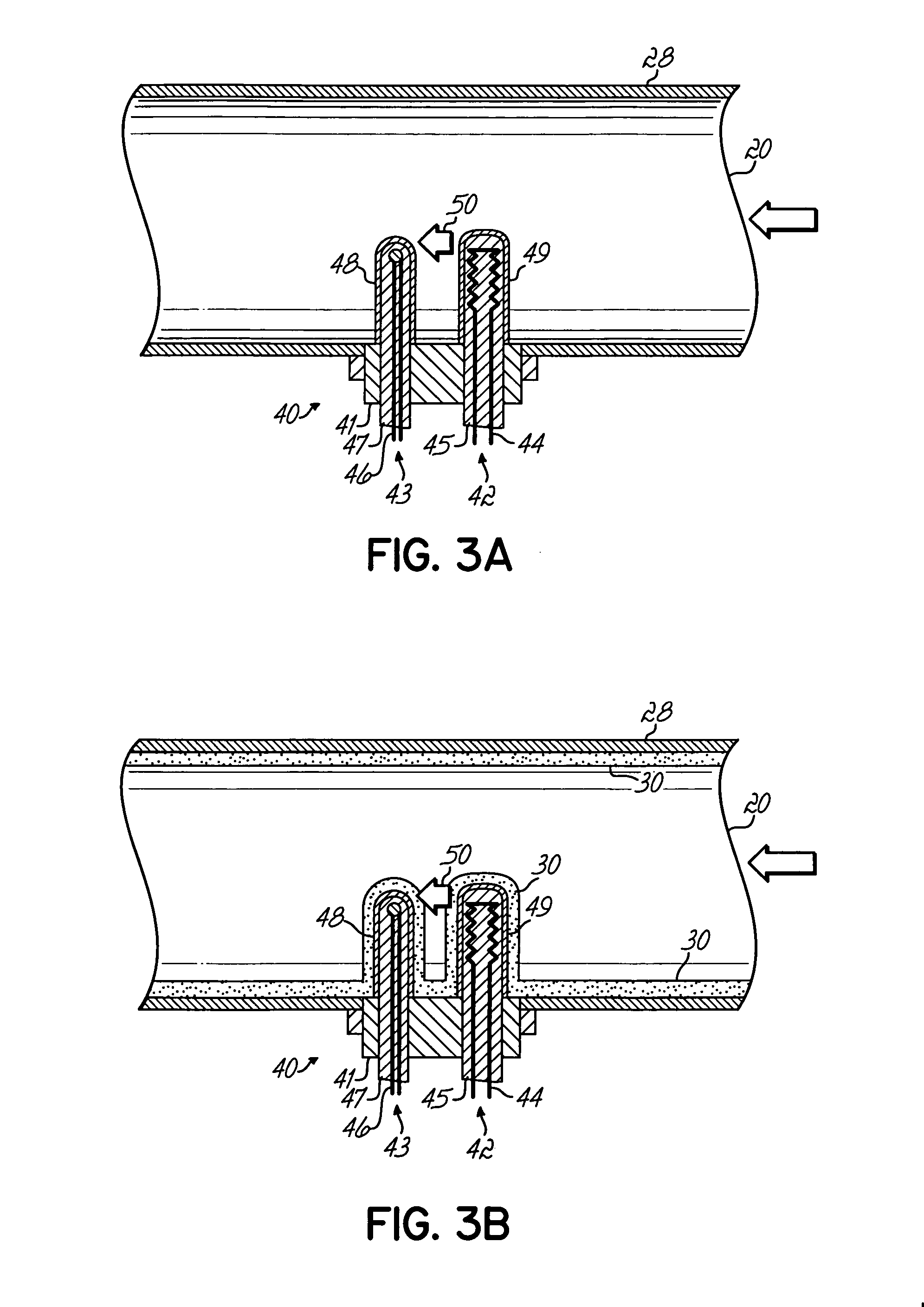
[0018] The exhaust system 16 of the semiconductor wafer processing system 10 includes an exhaust line 20 in which is connected a pressure controller 24 and a vacuum pump 26. A sect...


PUM

PropertyMeasurementUnit
thermal responseaaaaaaaaaa
thicknessaaaaaaaaaa
thermal profileaaaaaaaaaa

Abstract

A system is provided for determining when the buildup of deposits in an exhaust line of a semiconductor wafer processing machine requires cleaning. Deposits in vacuum exhaust lines build up to where they eventually fail structurally, releasing particles that can contaminate equipment and processes. The time at which cleaning is required is often unpredictable, while frequent or early cleaning to avoid waiting too long unnecessarily reduces productivity. The invention provides for the monitoring of thermal properties on the inside of an exhaust line wall. Deposits cause changes in the monitored thermal properties. A heater and thermocouple can be used, for example, and the temperature at the thermocouple that is due to heat flow from the heater is measured. Buildups in the exhaust line affect heat flow to the sensor and are measurable as a decline in sensed temperature. Structural failure of the coating in the exhaust line leads to the eventual leveling off and fluctuation of the temperature measurement. Comparison or correlation of the sensed thermal property or a profile thereof with data stored under known exhaust line conditions is used to determine the condition of the exhaust line and signal when cleaning is most appropriate.

Description

[0001] This invention relates to the reduction of particulate contamination in semiconductor processing and to the efficiency of such processing. BACKGROUND OF THE INVENTION [0002] In semiconductor manufacturing, deposition processes must usually be performed with a minimum of particle generation. One of the sources of particle generation can be from the physical failure or breakdown of the buildup within the exhaust line leading from a deposition or other processing apparatus. This buildup typically accumulates from the reaction of process by-products downstream of the process chamber over repeated process runs. If this buildup breaks down in the exhaust line, particles are generated. Some of these particles can move upstream during the cycling of the system or can contaminate the environment around the processing equipment that can lead to contamination entering other adjacent processing systems. [0003] To minimize or prevent failure of this buildup, a process exhaust line is typi...

Claims


Application Information

Patent Timeline
Patent Type & Authority Applications(United States)
IPC IPC(8): G01K3/00G01N25/00
CPCC23C16/4412C23C16/52H01L21/67288H01L21/67253H01L21/67248
Inventor PETTIT, JONATHANJOE, RAYMOND
Owner TOKYO ELECTRON LTD
Why Eureka
Try Eureka