

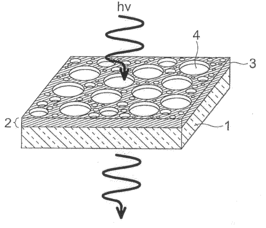
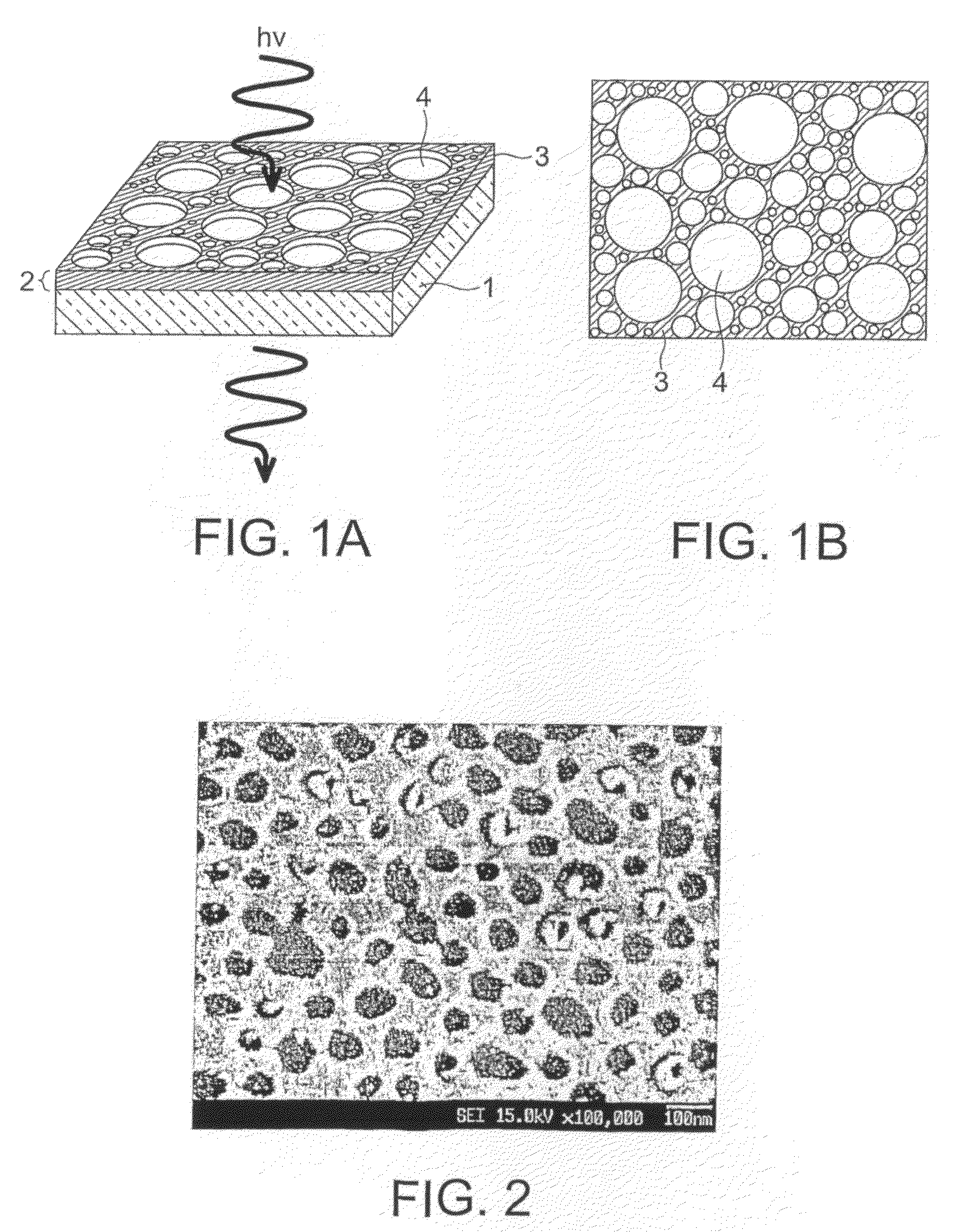
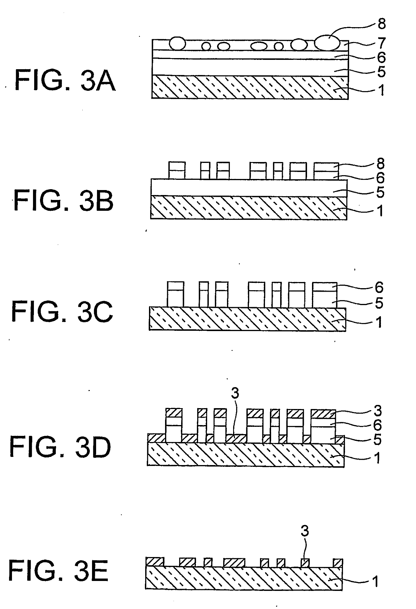
Solar cell and method for manufacturing metal electrode layer to be used in the solar cell
a technology of solar cells and metal electrodes, applied in the field of solar cells, can solve the problems of large production cost of transparent electrodes, low efficiency of crystalline si solar cells, and energy loss at the portions, and achieve the effect of low resistance and high transmission properties
- Summary
- Abstract
- Description
- Claims
- Application Information
AI Technical Summary
Benefits of technology
Problems solved by technology
Method used
Image

Examples
example 1
[0084]Example 1 concerns a method for manufacturing a single-crystal solar cell. FIG. 4 is a cross-sectional view of a single-crystal Si solar cell that includes an optically-transparent metal electrode layer having openings in accordance with the present invention.
[0085]As shown in FIG. 4, a p-type silicon substrate 9a that is p-type single-crystal silicon is first prepared as a semiconductor substrate. The p-type silicon substrate 9a is p-type single-crystal silicon that is formed by slicing a silicon ingot with a multi-wire saw into pieces of 230 μm in thickness. The silicon ingot is doped with boron and is lifted by the Czochralski method. The p-type single-crystal silicon is approximately 2 Ω·cm in specific resistance. The p-type silicon substrate 9a is then thinned to 70 μm through mechanical polishing, and outside diameter processing is performed so that the p-type silicon substrate 9a has a square surface 5-cm on a side.
[0086]An n+ layer 10a containing a large amount of an n...
example 2
[0099]Example 2 concerns a method for manufacturing a polycrystalline Si solar cell. FIG. 5 is a cross-sectional view of a polycrystalline Si solar cell that includes an optically-transparent metal electrode layer having openings in accordance with the present invention. The method for manufacturing the polycrystalline Si solar cell is almost the same as the method for manufacturing the single-crystal Si solar cell of Example 1.
[0100]As shown in FIG. 5, a p-type silicon substrate 9b that is 250-μm thick polycrystalline silicon cut out of an ingot with a multiwire saw is first formed. Etching and cleaning with NaOH are then performed on the layer that is mechanically damaged on its surface at the time of the ingot cutting. Through the etching and cleaning, a plate-like structure having a 5-cm square surface is formed. The p-type silicon substrate 9b is then placed in a diffusion furnace, and is heated in phosphorus oxychloride (POCl3) at 850° C. for 30 minutes. In this manner, phosph...
example 3
[0104]Example 3 concerns a method for manufacturing an amorphous Si solar cell. FIG. 6 is a cross-sectional view of the amorphous Si solar cell that includes the metal electrode layer having openings in accordance with the present invention.
[0105]The amorphous Si solar cell differs from any of the above described crystalline Si solar cells, in that the light absorption coefficient is large, and the absorption layer can be thinned. However, in a case where a pn junction is formed, carrier traps and recoupling are promptly caused due to structural defects and the likes in the amorphous Si. To counter those problems, an i-layer that is undoped Si on which doping is not performed is formed between a p-type Si layer and an n-type Si layer in the amorphous Si solar cell. The i layer absorbs light, and the carriers divided into holes and electrons reach the n-layer and the p-layer by virtue of the electric field induced in the i-layer. Those carriers then generate electromotive force. Also...
PUM
| Property | Measurement | Unit |
|---|---|---|
| thickness | aaaaa | aaaaa |
| width | aaaaa | aaaaa |
| width | aaaaa | aaaaa |
Abstract
Description
Claims
Application Information