

Photoelectric conversion device and solid-state imaging device
- Summary
- Abstract
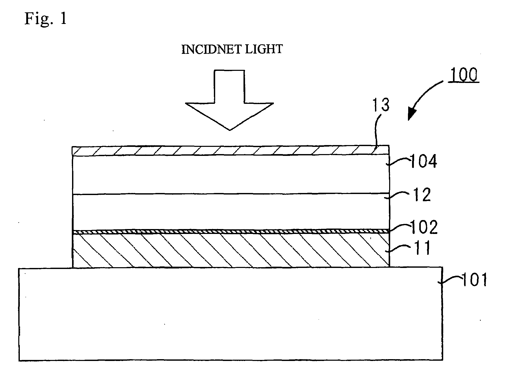
- Description
- Claims
- Application Information
AI Technical Summary
Benefits of technology
Problems solved by technology
Method used
Image

Examples
first configuration example
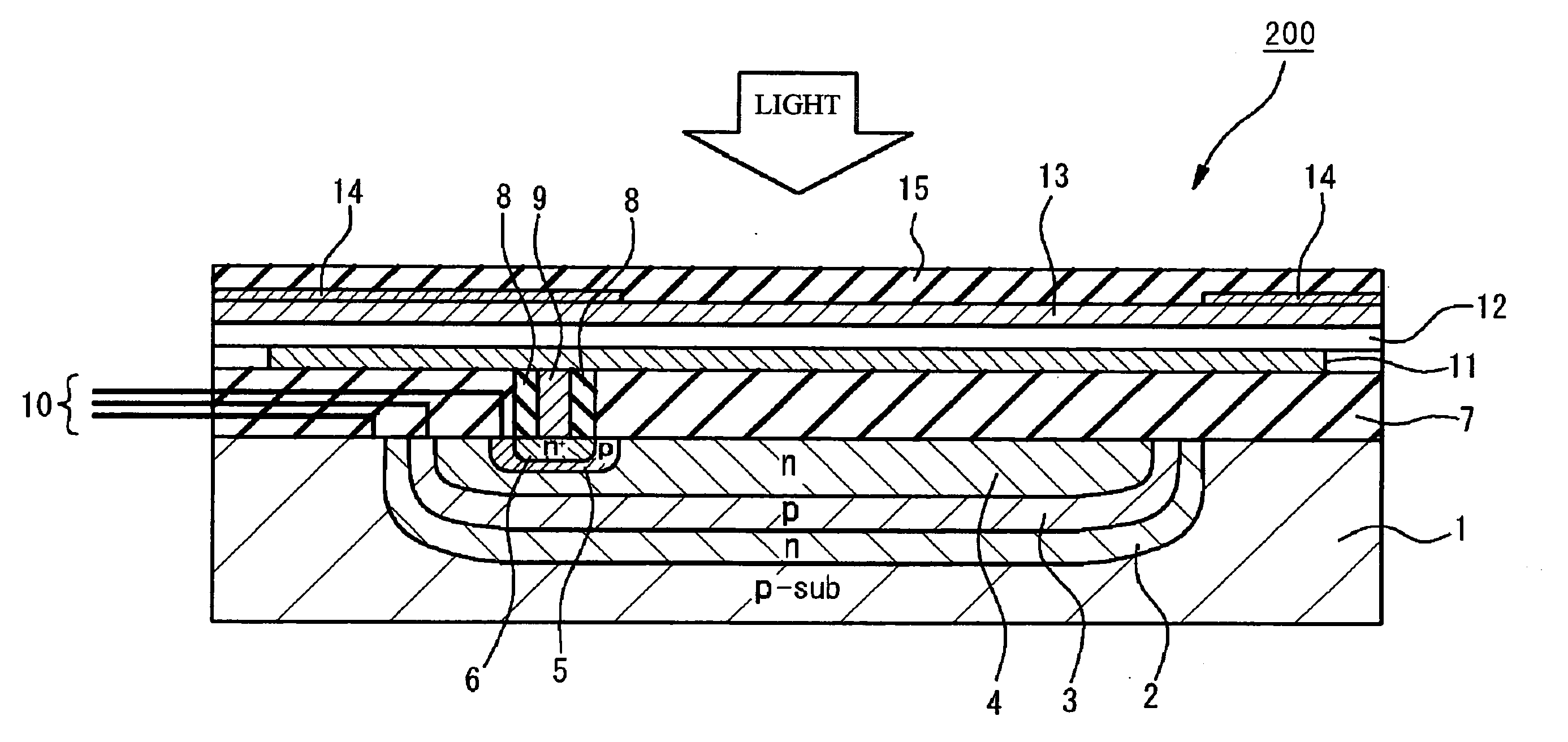
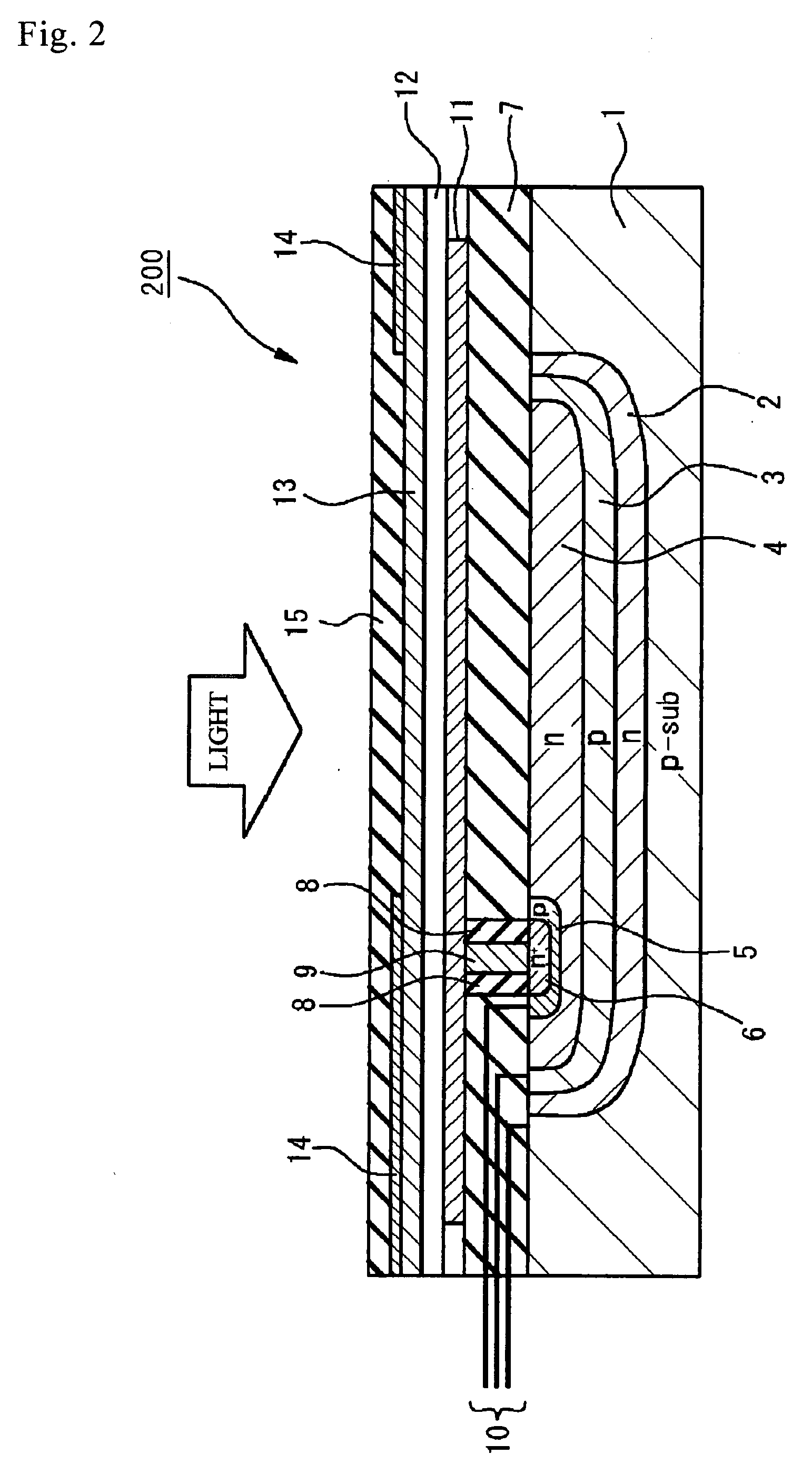
[0075]FIG. 2 is a sectional schematic view of a portion of one pixel of a solid-state imaging device using a photoelectric conversion device of the configuration as illustrated in FIG. 1 and is a view to show a first configuration example. In this solid-state imaging device 200, the one pixel as illustrated in FIG. 2 is disposed in a plural number in an array state on the same plane, and one pixel data of image data can be produced by a signal as obtained from this one pixel.
[0076]One pixel of the solid-state imaging device as illustrated in FIG. 2 is configured to have the photoelectric conversion part as illustrated in FIG. 1 and two photodiodes formed on a silicon substrate in a lower part of this photoelectric conversion part. In FIG. 2, symbols the same as in FIG. 1 are given the same symbols. Furthermore, the work function adjusting layer 102 and the smoothing layer 104 as illustrated in FIG. 1 are omitted from illustration.
[0077]One pixel of the solid-state imaging device as ...
second configuration example
[0093]In a second configuration example, the inorganic layer having the configuration as illustrated in FIG. 2 which is described in the first configuration example is prepared in such a manner that two photodiodes are not stacked within the p-type silicon substrate but that two photodiodes are arranged in a direction vertical to an incident direction of the incident light, thereby detecting lights of two colors within the p-type silicon substrate.
[0094]FIG. 3 is a sectional schematic view of a portion of one pixel of a solid-state imaging device using the photoelectric conversion device having the configuration as illustrated in FIG. 1 and is a view to show a second configuration example. In FIG. 3, configurations the same as in FIG. 2 are given the same symbols.
[0095]One pixel of a solid-state imaging device 300 as illustrated in FIG. 3 is configured to include a p-type silicon substrate 17 and a photoelectric conversion part formed in an upper part of the p-type silicon substrate...
third configuration example
[0106]A third configuration example is concerned with a configuration in which the inorganic layer having the configuration as illustrated in FIG. 2 which is described in the first configuration example is not provided and the photoelectric conversion layer having the configuration as illustrated in FIG. 1 is stacked in a plural number (three in this instance) in an upper part of the silicon substrate.
[0107]FIG. 4 is a sectional schematic view of a portion of one pixel of a solid-state imaging device using the photoelectric conversion device having the configuration as illustrated in FIG. 1 and is a view to show a third configuration example. FIG. 4 shows a configuration example in which a photoelectric conversion part for detecting G light, a photoelectric conversion part for detecting R light and a photoelectric conversion part for detecting B light are stacked as the photoelectric conversion part. Though each of the photoelectric conversion parts has a configuration the same as t...
PUM
 Abstract
Description
Claims
Application Information