Semiconductor memory and method for manufacturing a semiconductor memory

a semiconductor memory and semiconductor technology, applied in semiconductor devices, digital storage, instruments, etc., can solve the problems of increasing the capacitance between the floating gate electrode narrowing the distance between the adjacent gate electrodes, and difficult to arrange the inter-electrode insulating film and the control gate electrode, so as to reduce the gate capacitance and drive the floating gate electrode efficiently.

Inactive Publication Date: 2007-08-23
KK TOSHIBA
View PDF16 Cites 15 Cited by
  • Summary
  • Abstract
  • Description
  • Claims
  • Application Information

AI Technical Summary

Benefits of technology

[0010] The present invention provides a semiconductor memory and a method for manufacturing a semiconductor memory, which can efficiently drive a floating gate electrode, and can decrease a gate capacitance.

Problems solved by technology

However, as the memory cell transistor has continued to be integrated / miniaturized, the distance between the adjacent gate electrodes has become more narrow.
Therefore, it has become difficult to arrange the inter-electrode insulating film and the control gate electrode between the adjacent floating gate electrodes.
Hence, it has become difficult to increase the capacitance between the floating gate electrode and the control gate electrode more than the capacitance between the floating gate electrode and the channel region.
Owing to an influence from the capacitance between the adjacent gates, a threshold value of the memory cell transistor in which writing operation is not performed is varied, sometimes resulting in deterioration of write accuracy.

Method used


Image

  • Semiconductor memory and method for manufacturing a semiconductor memory
  • Semiconductor memory and method for manufacturing a semiconductor memory
  • Semiconductor memory and method for manufacturing a semiconductor memory

Examples


first modification

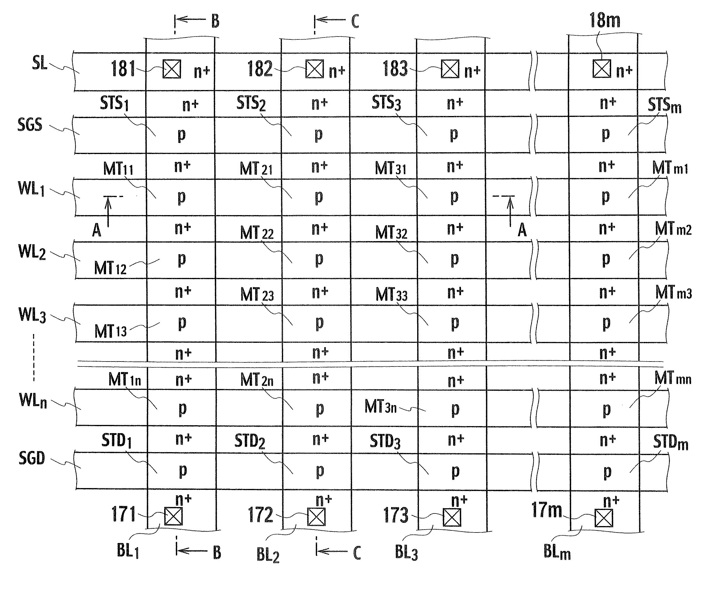
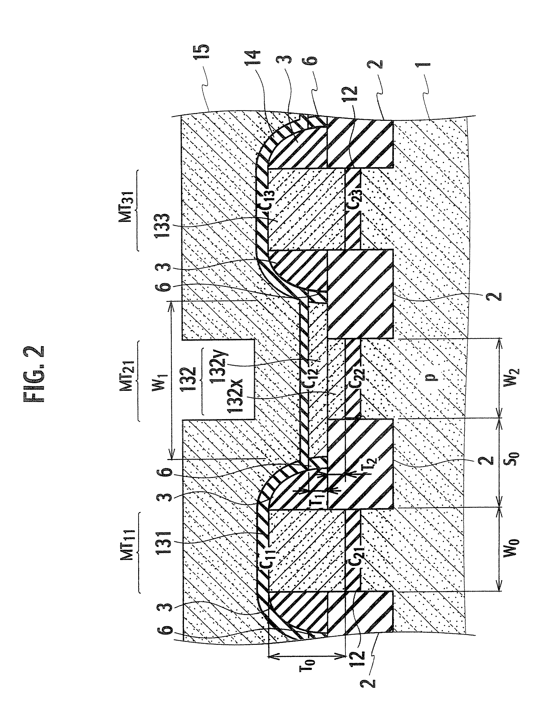
[0144] In the embodiment of the present invention, the description has been made of the case where the floating gate electrode 132 shown in FIG. 1 has a T-shaped (convex) cross-sectional shape; however, the shape of the second floating gate 132 is not particularly limited. In a first comparison, a description will be made of an example of another shape of the second floating gate electrode 132.

[0145] For example, as shown in FIG. 43, the cross-sectional shape of the second floating gate electrode 132 in the row direction may be a hook shape (L-shape). The second floating gate electrode 132 includes the lower member 132x having the width W2, and the upper member 132y having a width W3, which is wider than the width W2 and disposed on the lower member 132x. With regard to a method of forming the second floating gate electrode 132 shown in FIG. 43, for example, it is satisfactory if the mask film is formed on a part of the upper surface of the upper member 132y shown in FIGS. 36A and ...

second modification

[0151] An example of a method for manufacturing a non-volatile semiconductor memory according to a second modification of the embodiment of the present invention will be described, referring to FIGS. 48 to 54. FIGS. 48 to 54 are cross-sectional views in the row direction, taken along the A-A line of FIG. 1.

[0152] After the element isolation insulating film 2 is deposited as shown in FIG. 27B, the element isolation insulating film 2 is etched back by chemical mechanical polishing (CMP), and the mask film 4 is also removed. As a result, as shown in FIG. 48, the upper surfaces of the first floating gate layers 131 and 133 and the second floating gate layer 132x and the upper surface of the element isolation insulating film 2 are horizontally aligned with each other. The mask film 10 is deposited by CVD and the like on the upper surfaces of the first floating gate layers 131 and 133, the second floating gate layer 132x, and the element isolation insulating film 2. A resist film is spin...


PUM


Abstract

A semiconductor memory includes: a first memory cell transistor including: a first floating gate electrode provided on and insulated from the substrate; and a first control gate electrode provided on and insulated from the first floating gate electrode; and a second memory cell transistor including: a second floating gate electrode provided on and insulated from the substrate, an upper surface being larger than a lower surface, and the upper surface being lower than an upper surface of the first floating gate electrode; and a second control gate electrode provided on and insulated from the second floating gate electrode.

Description

CROSS REFERENCE TO RELATED APPLICATIONS AND INCORPORATED BY REFERENCE [0001] The application is based upon and claims the benefit of priority from the prior Japanese Patent Applications No. P2006-045934, filed on Feb. 22, 2006; the entire contents of which are incorporated herein by reference. BACKGROUND OF THE INVENTION [0002] 1. Field of the Invention [0003] This present invention relates to a semiconductor memory and a method for manufacturing a semiconductor memory. [0004] 2. Description of the Related Art [0005] An electrically erasable programmable read-only memory (EEPROM) is known as a non-volatile semiconductor memory. In the EEPROM, a cell array is configured in such a way that a memory cell transistor is arranged at an intersection where a word line in the row direction and a bit line in the column direction cross over each other. Among the various EEPROMs, the NAND flash EEPROM in which a plurality of memory cell transistors are connected in series, and which can erase a...

Claims


Application Information

Patent Timeline
Patent Type & Authority Applications(United States)
IPC IPC(8): G06F12/00
CPCG11C11/5628G11C16/0483H01L27/11524H01L27/11521H01L27/115H10B69/00H10B41/30H10B41/35H10B63/80
Inventor MIZUKAMI, MAKOTOKINOSHITATAKAGI, SHIGEYUKI
Owner KK TOSHIBA
Why Eureka
Try Eureka