Top-emitter OLED device structure and method

Active Publication Date: 2007-08-30
GLOBAL OLED TECH
View PDF19 Cites 203 Cited by
  • Summary
  • Abstract
  • Description
  • Claims
  • Application Information

AI Technical Summary

Benefits of technology

[0025] The present invention has the advantage that it impr

Problems solved by technology

Such unpatterned, common light-emitters may be preferred since patterning colored emitters can be difficult.
However, such designs are relatively inefficient since approximately two-thirds of the light emitted may be absorbed by the color filters.
It has also been found, that one of the key factors that limits the efficiency of OLED devices is the inefficiency in extracting the photons generated by the electron-hole recombination out of the OLED devices.
Due to the high optical indices of the organic materials used, most of the photons generated by the recombination process are actually trapped in the devices due to total internal reflection.
In general, up to 80% of the light may be lost in this manner.
However, none of these approaches cause all, or nearly all, of the light produced to be emitted from the device.
Moreover, such diffractive techniques cause a significant frequency dependence on the angle of emission so that the color of the light emitted from the device changes with the viewer's perspective.
While useful for ex

Method used


Image

  • Top-emitter OLED device structure and method
  • Top-emitter OLED device structure and method
  • Top-emitter OLED device structure and method

Examples


Embodiment Construction

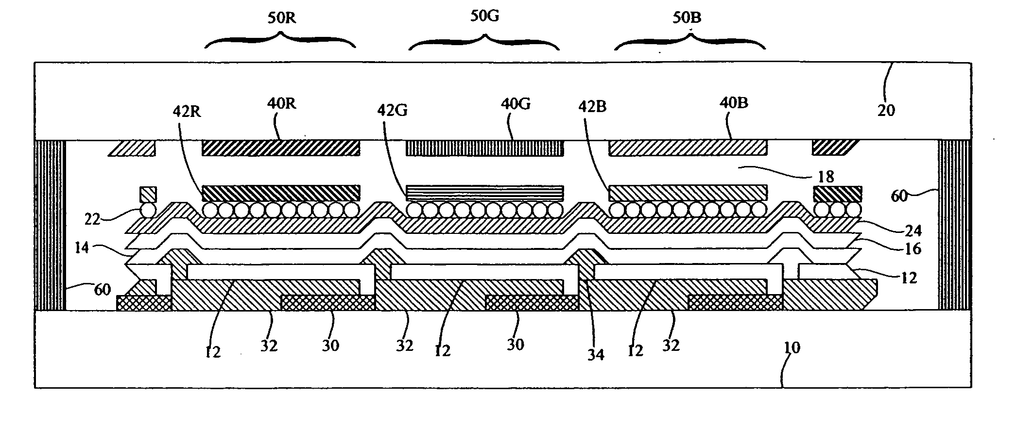
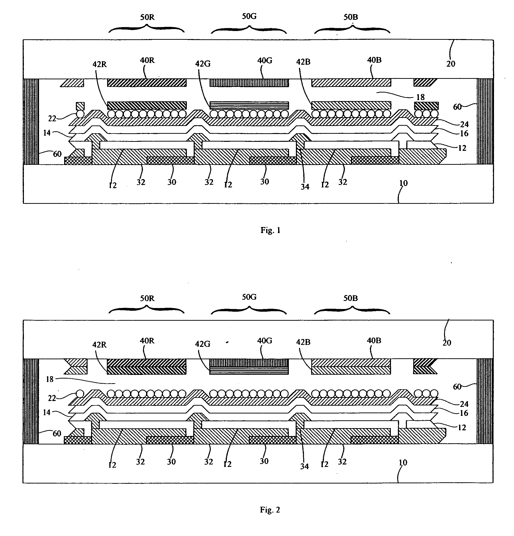
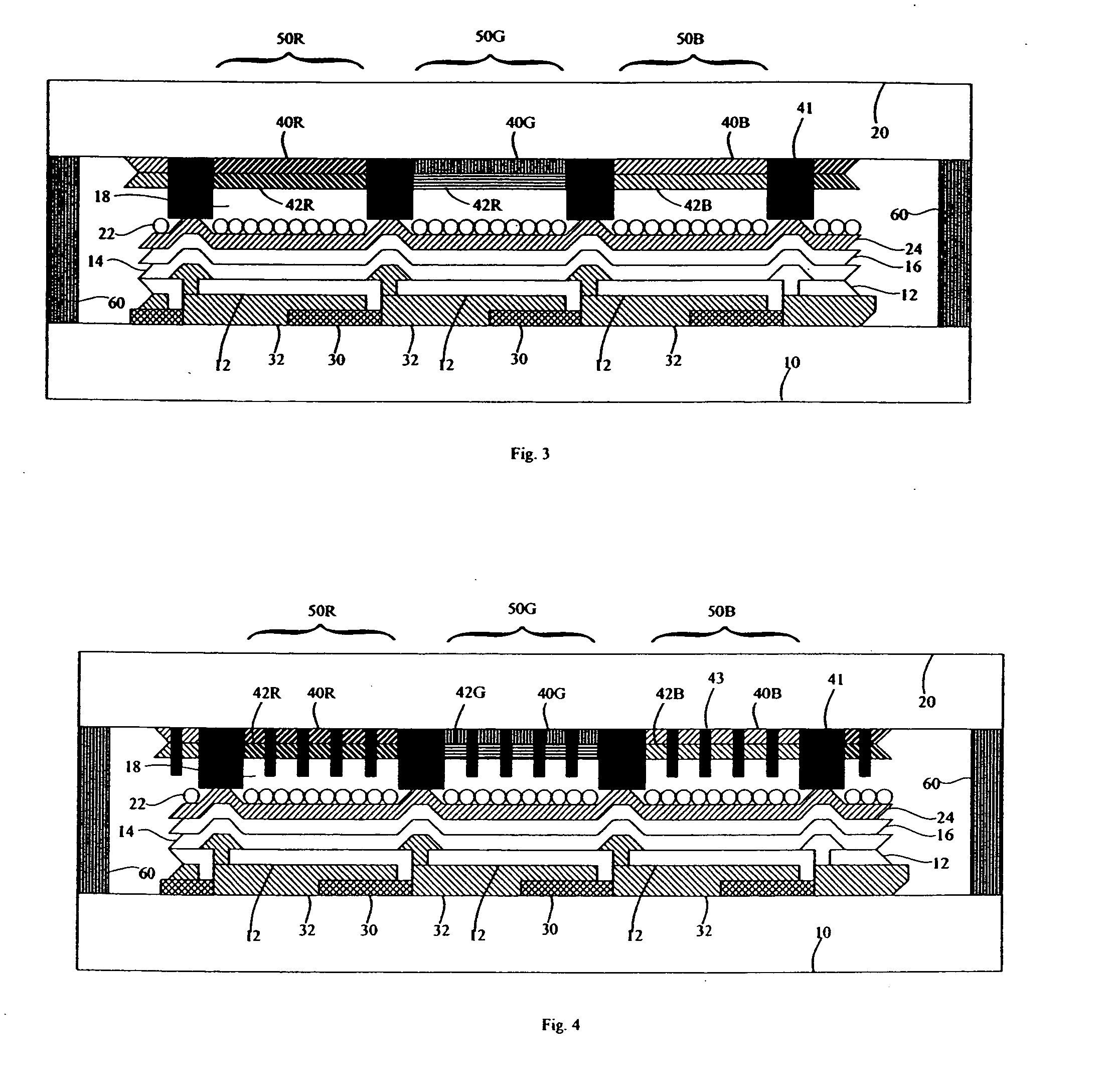
[0036] Referring to FIGS. 1 and 2, according to various embodiments of the present invention, a top-emitting OLED device comprises one or more OLEDs formed on a substrate 10, the OLED including a first electrode 12 formed over the substrate 10, one or more layers 14 of light-emitting organic material formed over the first electrode 12, and a transparent second electrode 16 formed over the one or more layers 14 of light-emitting organic material; a light-scattering layer 22 formed over the one or more OLEDs for scattering light emitted by the one or more layers 14 of light-emitting organic material; a transparent cover 20; one or more color filters 40 formed on the transparent cover 20; a color-conversion material layer 42 formed over the color filters 40 (FIG. 2) or the light-scattering layer 22 (FIG. 1); wherein the substrate 10 is aligned and affixed to the transparent cover 20 so that the locations of the color filters 40 and color conversion material 42 correspond to the locatio...


PUM


Abstract

A top-emitting OLED device, comprising: one or more OLEDs formed on a substrate; a light-scattering layer formed over the one or more OLEDs; a transparent cover; one or more color filters formed on the transparent cover; a color-conversion material layer formed over the color filters, or formed over or integral with the light-scattering layer; wherein the substrate is aligned and affixed to the transparent cover so that the locations of the color filters and color conversion material correspond to the location of the OLEDs, and the color-conversion material layer, color filters, and the light-scattering layer are between the cover and substrate, and a low-index gap is formed between the light-scattering layer and the color filters, with no light-scattering layer being positioned between the color conversion material layer and the low-index gap.

Description

FIELD OF THE INVENTION [0001] The present invention relates to OLED devices, and more particularly, to top-emitter OLED devices having improved efficiency and reduced manufacturing costs. BACKGROUND OF THE INVENTION [0002] Flat-panel display devices employ a variety of technologies for emitting patterned, colored light to form full-color pixels. Some of these technologies employ a common light-emitter for all of the color pixels and color-conversion materials to convert the light of the common light-emitter into colored light of the desired frequencies. Such unpatterned, common light-emitters may be preferred since patterning colored emitters can be difficult. For example, liquid crystal displays (LCDs) typically employ a backlight that relies on either fluorescent tubes to emit a white light or a set of differently colored, inorganic light-emitting diodes to emit white light together with patterned color filters, for example red, green, and blue, to create a full-color display. It ...

Claims


Application Information

Patent Timeline
IPC IPC(8): H01J1/62H01J63/04
CPCH01L27/322H01L51/5237H01L2251/5315H01L51/5284H01L51/5268H10K59/38H10K50/8428H10K50/854H10K50/844H10K50/865H10K2102/3026
Inventor COK, RONALD S.ARNOLD, ANDREW D.BURBERRY, MITCHELL S.
Owner GLOBAL OLED TECH
Why Eureka
Try Eureka