Solid-state image sensing device having photoelectric conversion cells each configured by n pixels in vertical direction

Inactive Publication Date: 2007-08-30
KK TOSHIBA
View PDF5 Cites 7 Cited by
  • Summary
  • Abstract
  • Description
  • Claims
  • Application Information

AI Technical Summary

Problems solved by technology

Therefore, a lowering in the sensitivity becomes significant and the image quality at low illumination is greatly degraded.
However, if the vertical-2-pixel / one-cell structure is made, the photodiodes cannot be arranged at uniform intervals because the separation state between the photodiodes becomes non-uniform, for example.
Therefore, coloring tends to occur in the upper portion or lower portion of the output screen due to chromatic aberration of the optical lens even in the one-pixel-one-cell structure in which the photodiodes are not commonly used.

Method used


Image

  • Solid-state image sensing device having photoelectric conversion cells each configured by n pixels in vertical direction
  • Solid-state image sensing device having photoelectric conversion cells each configured by n pixels in vertical direction
  • Solid-state image sensing device having photoelectric conversion cells each configured by n pixels in vertical direction

Examples


first embodiment

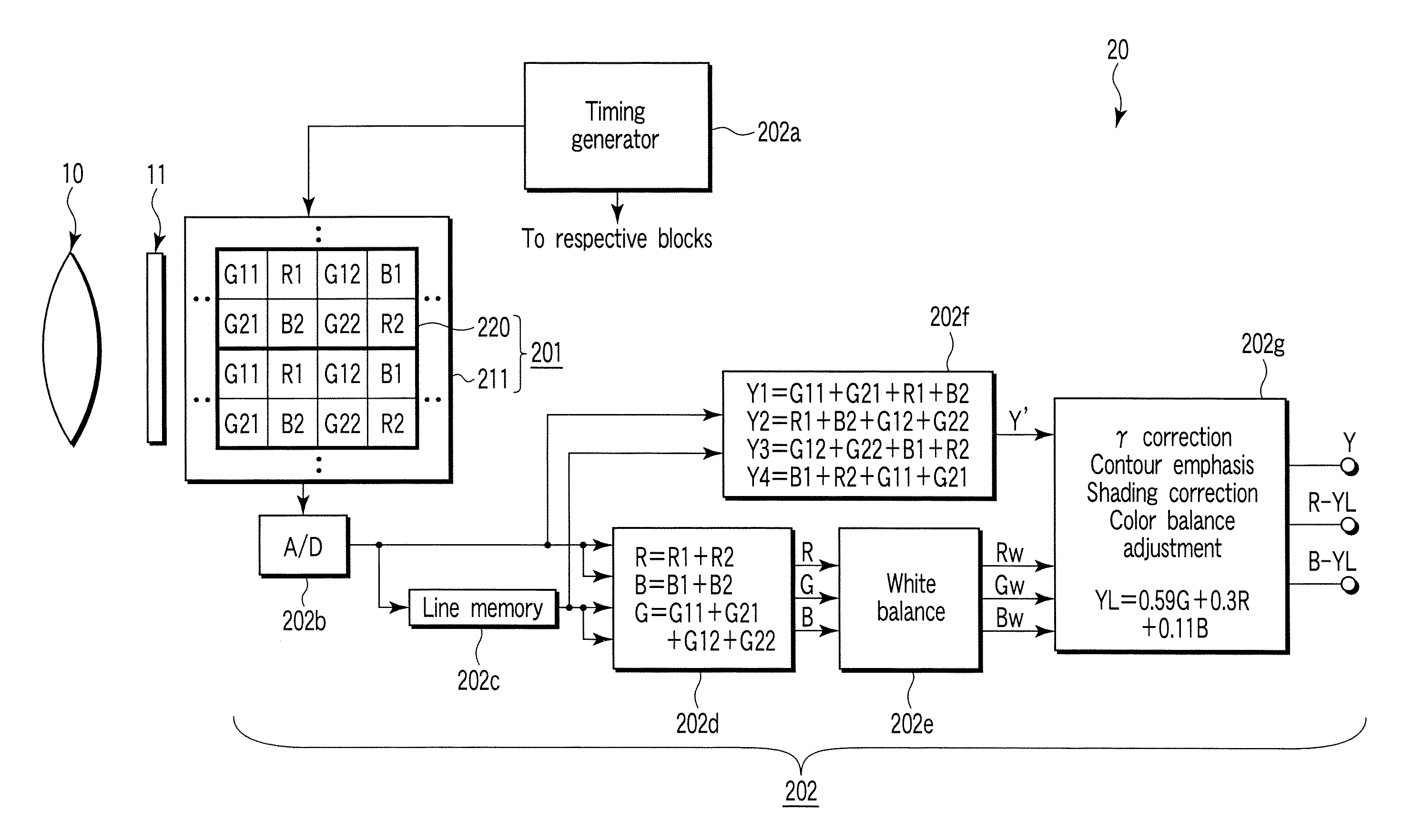
[0025]FIG. 1 shows the basic configuration of a one-chip camera such as a digital camera or video camera using a CMOS type color image sensor (solid-state image sensing device) according to a first embodiment of this invention. In this example, a case wherein primary color filters of red (R), green (G) and blue (B) are used as color filters is explained.

[0026] As shown in FIG. 1, the one-chip camera includes an optical lens (image sensing optical system) 10, infrared-cut filter 11 and amplification type CMOS color image sensor 20. The infrared-cut filter 11 is used to cut or omit infrared light contained in light emitted from the optical lens 10.

[0027] The image sensor 20 is configured by a solid-state image sensing device 201 and signal processor 202 mounted on one chip, for example. On a pixel area 211 of the solid-state image sensing device 201, a plurality of color filters 220 of three primary colors are arranged in a two-dimensional form. Each of the color filters 220 has the...

second embodiment

[0056]FIG. 7 showing the basic configuration of a one-chip camera using a CMOS type color image sensor (solid-state image sensing device) according to a second embodiment of this invention. In this example, a case wherein the photoelectric conversion cell is formed with the vertical-2-pixel / one-cell structure and a complementary color filter of white / transparent (W), cyan (Cy), yellow (Ye) is used as a color filter is explained. Portions which are the same as those of FIG. 1 are denoted by the same reference symbols and the detail explanation thereof is omitted.

[0057] As shown in FIG. 7, in the present embodiment, the array of a color filter 221 is formed in a W-stripe / CyYe complete checkered form having the area corresponding to eight pixels of W, Cy, Ye in total area with two pixels in the vertical (row) direction and four pixels in the horizontal (column) direction. That is, in the case of the present embodiment, for example, W11 and W12 filters of a first color are respectively...

third embodiment

[0062]FIG. 8 shows the basic configuration of a one-chip camera using a CMOS type color image sensor (solid-state image sensing device) according to a third embodiment of this invention. In this example, a case wherein a photoelectric conversion cell is formed with the vertical-2-pixel / one-cell structure and a color filter of white / transparent (W), red (R), blue (B) is used as a color filter is explained. Portions which are the same as those of FIG. 1 are denoted by the same reference symbols and the detail explanation thereof is omitted.

[0063] As shown in FIG. 8, in the present embodiment, the array of a color filter 222 is formed in a W-stripe / RB complete checkered form having the size corresponding to eight pixels of W, R, B in total including two pixels in the vertical (row) direction x four pixels in the horizontal (column) direction. That is, in the case of the present embodiment, for example, W11 and W12 filters of a first color are respectively arranged on the first and thi...


PUM


Abstract

A solid-state image sensing device includes a plurality of color filters. Each of the plurality of color filters is configured to have two pixels in a vertical direction and four pixels in a horizontal direction of a plurality of light receivers used as one unit area, a first color is arranged on first and third pixels in the horizontal direction of a first line in the vertical direction, a second color is arranged on a second pixel in the horizontal direction, a third color is arranged on a fourth pixel in the horizontal direction, the first color is arranged on first and third pixels in the horizontal direction of a second line in the vertical direction, the third color is arranged on a second pixel in the horizontal direction and the second color is arranged on a fourth pixel in the horizontal direction.

Description

CROSS-REFERENCE TO RELATED APPLICATIONS [0001] This application is based upon and claims the benefit of priority from prior Japanese Patent Application No. 2006-053298, filed Feb. 28, 2006, the entire contents of which are incorporated herein by reference. BACKGROUND OF THE INVENTION [0002] 1. Field of the Invention [0003] This invention relates to a solid-state image sensing device and more particularly to a complementary metal oxide semiconductor (CMOS) type color image sensor used in a mobile telephone with a camera, digital camera or video camera. [0004] 2. Description of the Related Art [0005] Recently, in most of charge coupled device (CCD) type and CMOS type color image sensors, primary color filters which are excellent in color reproducibility are arranged in Bayer pattern. In the case of an image sensor used in a digital camera or mobile telephone, pixels with the pixel size equal to or slightly larger than 2 μm are mainly used in order to increase the number of pixels. At ...

Claims


Application Information

Patent Timeline
IPC IPC(8): H04N1/46
CPCH04N1/46H01L27/146
InventorEGAWA, YOSHITAKA
OwnerKK TOSHIBA