Cell-Downgrading and Reference-Voltage Adjustment for a Multi-Bit-Cell Flash Memory

Inactive Publication Date: 2007-08-30
SUPER TALENT TECH CORP
View PDF14 Cites 142 Cited by
  • Summary
  • Abstract
  • Description
  • Claims
  • Application Information

AI Technical Summary

Problems solved by technology

However, since flash memory chips are block-addressable rather than randomly-accessible, flash is not as easy to use for a cache as DRAM or SRAM.
However, MLC flash chips may impose additional restrictions on usage.
For example, a MLC flash chip may not allow pages to be written a second time before erase.
Some MLC flash chips may be even more restrictive, only allowing pages to be written in a sequence within a block, and not allowing pages to be written out-of-order.
Another problem with MLC cells, especially with many states per cell, is that the noise margins are very small.
Over time

Method used


Image

  • Cell-Downgrading and Reference-Voltage Adjustment for a Multi-Bit-Cell Flash Memory
  • Cell-Downgrading and Reference-Voltage Adjustment for a Multi-Bit-Cell Flash Memory
  • Cell-Downgrading and Reference-Voltage Adjustment for a Multi-Bit-Cell Flash Memory

Examples


Embodiment Construction

[0032] The present invention relates to an improvement in flash-memory managers. The following description is presented to enable one of ordinary skill in the art to make and use the invention as provided in the context of a particular application and its requirements. Various modifications to the preferred embodiment will be apparent to those with skill in the art, and the general principles defined herein may be applied to other embodiments. Therefore, the present invention is not intended to be limited to the particular embodiments shown and described, but is to be accorded the widest scope consistent with the principles and novel features herein disclosed.

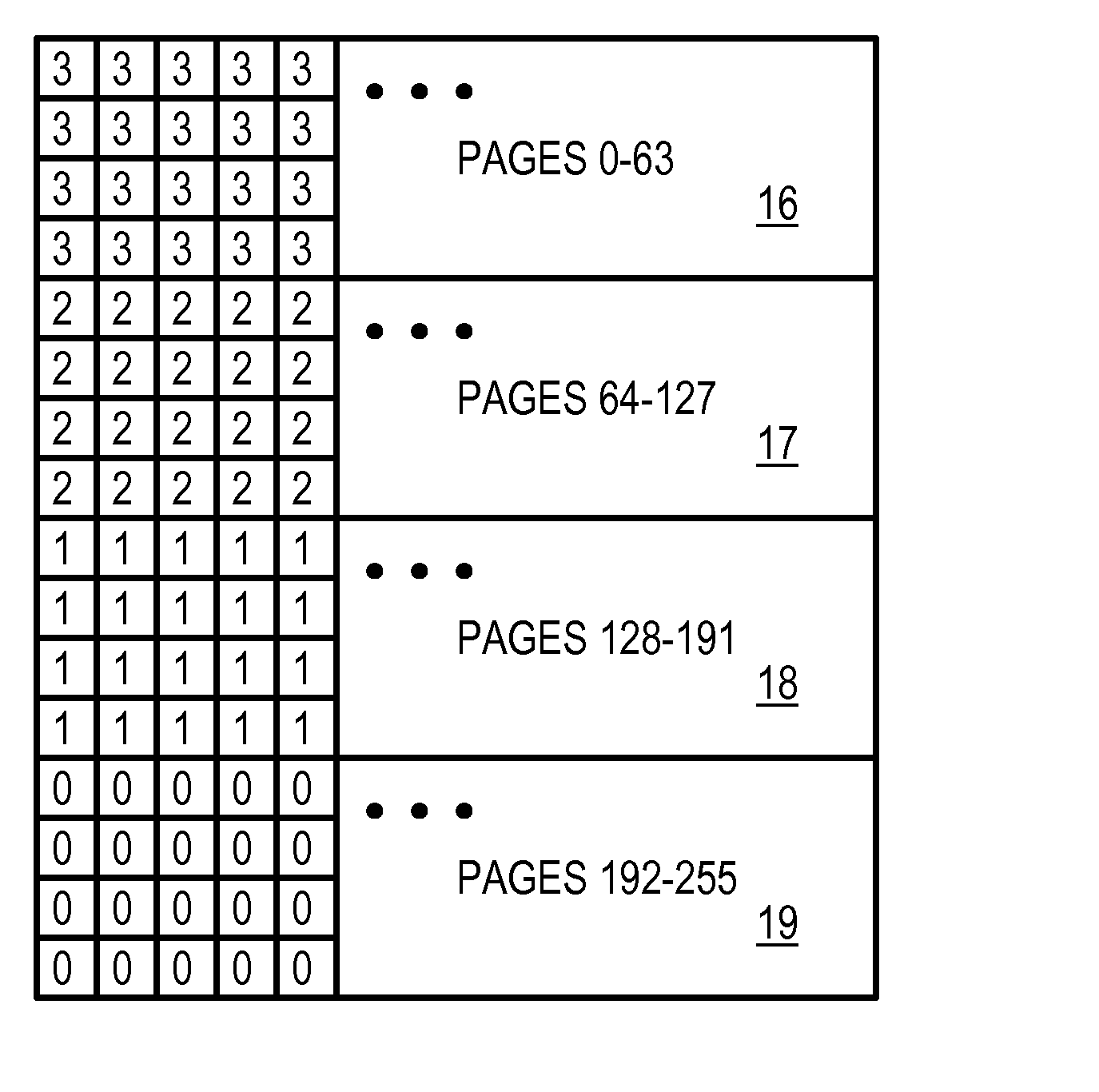
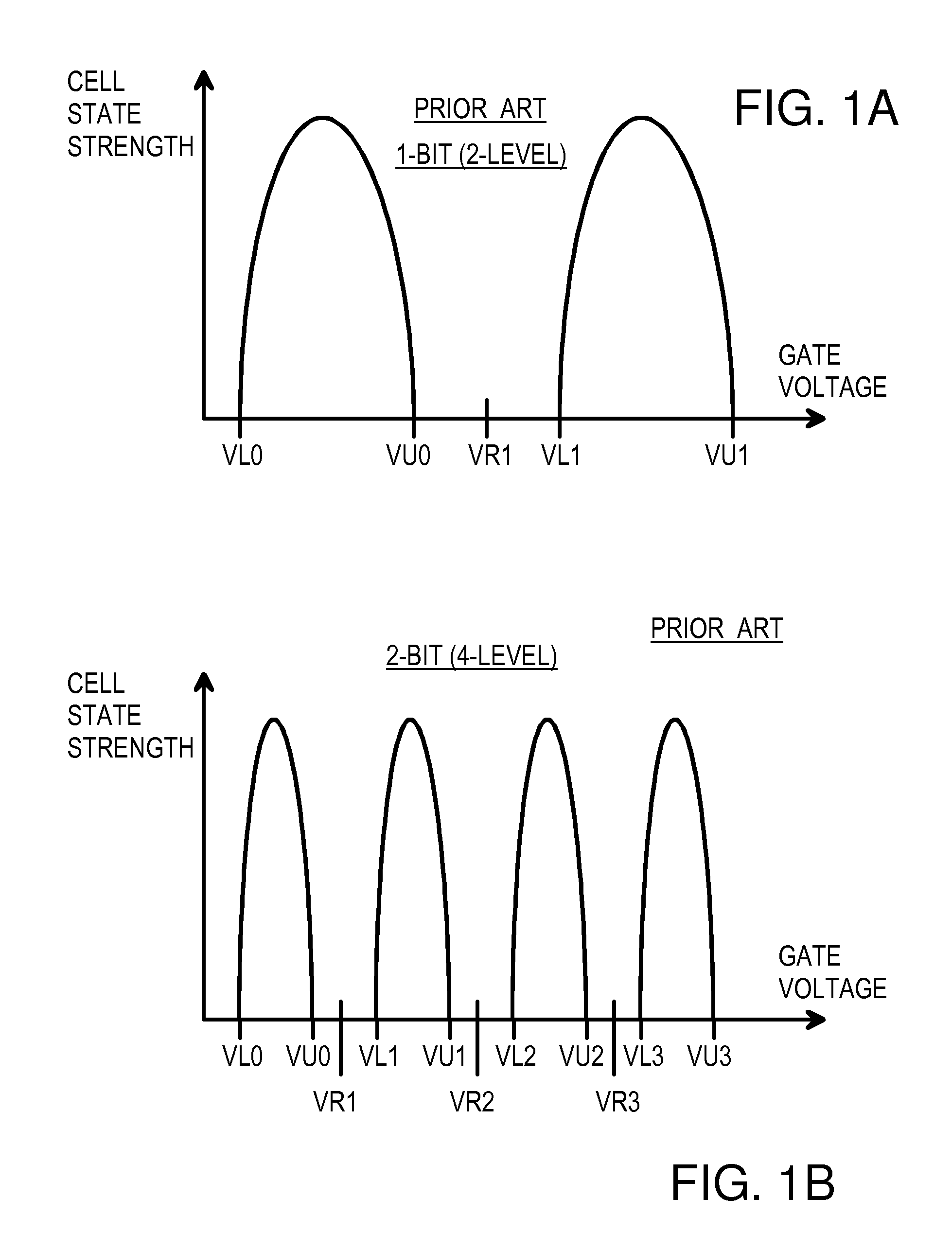
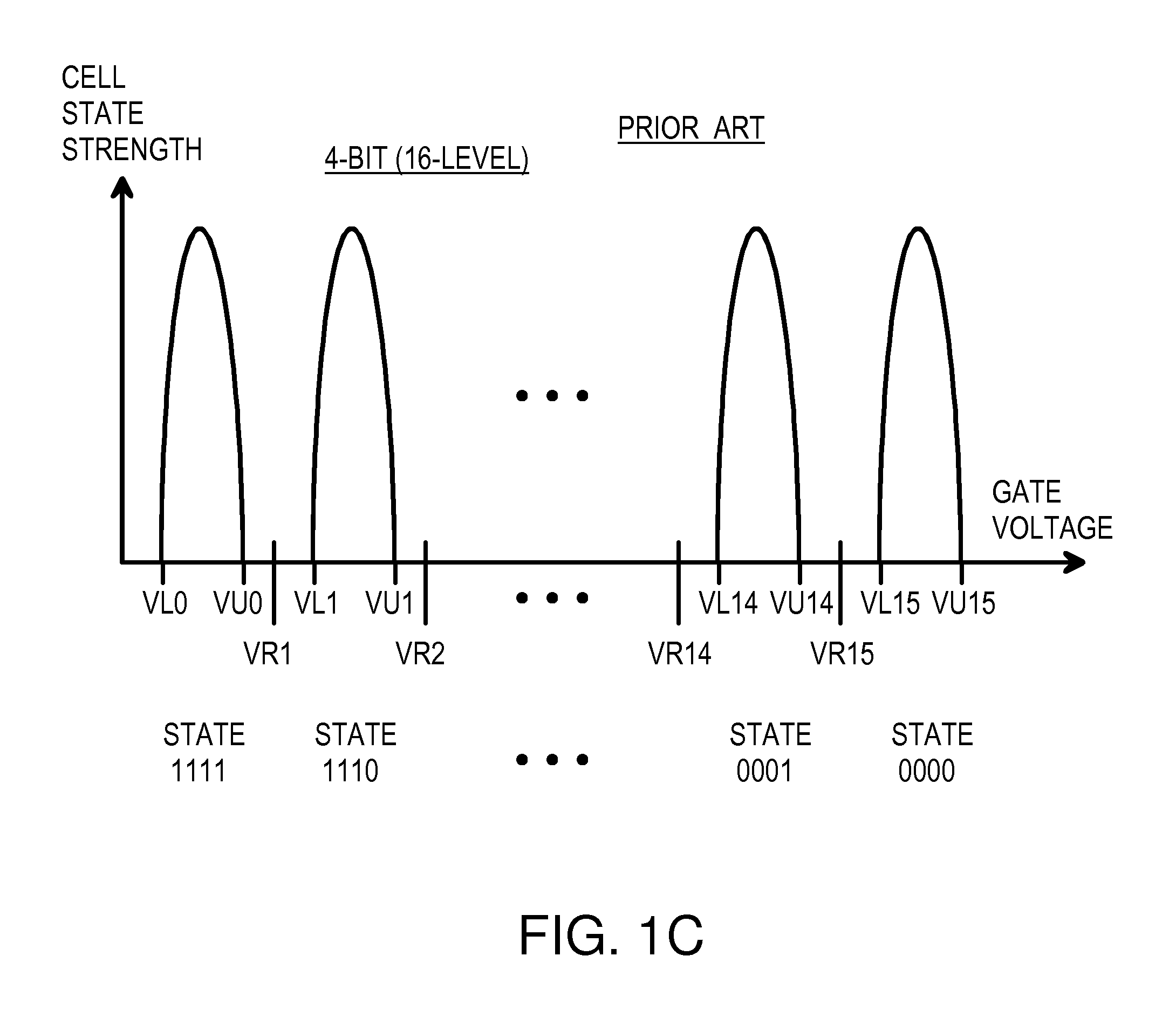
[0033] FIGS. 2A-B shown arrangements of multiple bits per flash cell. In FIG. 2A, all 4 bits in a single 16-level flash cell are arranged sequentially in the same flash page. Flash page 10 is a 2K-byte page that also has 64 ‘spare’ bytes for ECC, overhead, and management purposes. Since each 16-level flash cell represents four...


PUM


Abstract

A flash memory has multi-level cells (MLC) that can each store multiple bits per cell. Blocks of cells can be downgraded to fewer bits/cell when errors occur, or for storing critical data such as boot code. The bits from a single MLC are partitioned among multiple pages to improve error correctability using Error Correction Code (ECC). An upper reference voltage is generated by a voltage reference generator in response to calibration registers that can be programmed to alter the upper reference voltage. A series of decreasing references are generated from the upper reference voltage and are compared to a bit-line voltage. Compare results are translated by translation logic that generates read data and over- and under-programming signals. Downgraded cells use the same truth table but generate fewer read data bits. Noise margins are asymmetrically improved by using the same sub-states for reading downgraded and full-density MLC cells.

Description

RELATED APPLICATION [0001] This application is a continuation-in-part of the co-pending application for “Electronic Data Storage Medium with Fingerprint Verification Capability”, U.S. Ser. No. 09 / 478,720, filed Jan. 06, 2000, and “Flash Memory Controller for Electronic Data Flash Card” U.S. Ser. No. 11 / 466,759, filed Aug. 23, 2006, which is a CIP of “System and Method for Controlling Flash Memory”, U.S. Ser. No. 10 / 789,333, filed Feb. 26, 2004, now abandoned. [0002] This application is related to “Flash memory device and architecture with multi level cells”, U.S. Ser No. 10 / 800,228, filed Mar. 12, 2004, now U.S. Pat. No. 7,082,056, and “Flash drive / reader with serial-port controller and flash-memory controller mastering a second RAM-buffer bus parallel to a CPU bus”, U.S. Ser. No. 10 / 605,140, filed Sept. 10, 2003, now U.S. Pat. No. 6,874,044.FIELD OF THE INVENTION [0003] This invention relates to multi-bit-cell (MBC) or multi-level-cell (MLC) flash-memory systems, and more particula...

Claims


Application Information

Patent Timeline
IPC IPC(8): G11C11/34
CPCG11C11/5621G11C11/5642G11C2211/5641G11C2211/5634G11C29/00
Inventor YU, FRANKLEE, CHARLES C.MA, ABRAHAM C.SHEN, MING-SHIANG
Owner SUPER TALENT TECH CORP
Why Eureka
Try Eureka