Shift register and image display apparatus containing the same

Inactive Publication Date: 2007-09-20
TRIVALE TECH LLC
View PDF9 Cites 76 Cited by
  • Summary
  • Abstract
  • Description
  • Claims
  • Application Information

AI Technical Summary

Benefits of technology

[0012]An object of the present invention is to prevent malfunctions of shift registers

Problems solved by technology

Conversely, an a-Si TFT tends to have its threshold voltage shifted in the positive direction when the gate electrode is continuously positively biased (dc-biased), resulting in degraded driving capability (current-flowing capability).
Then, the output pull-down transistor cannot discharge unnecessary charges when supplied to the output terminal due to noise or

Method used


Image

  • Shift register and image display apparatus containing the same
  • Shift register and image display apparatus containing the same
  • Shift register and image display apparatus containing the same

Examples


first preferred embodiment

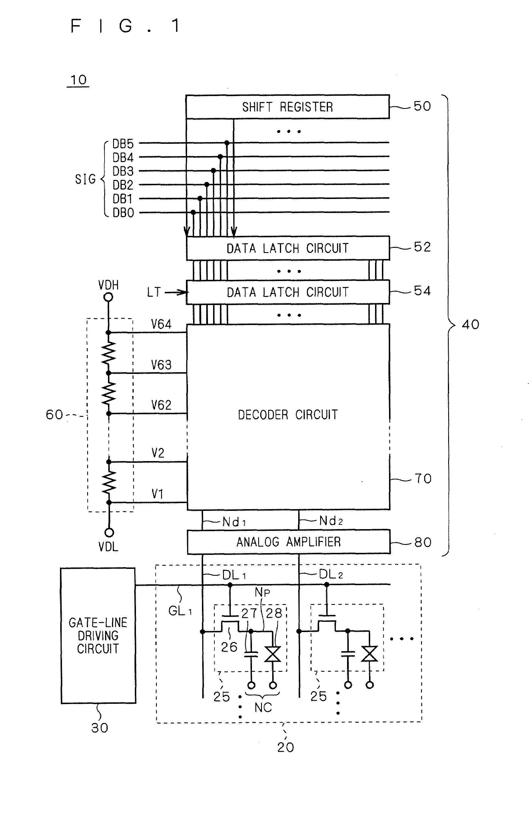
[0034]FIG. 1 is a schematic block diagram illustrating the configuration of a display apparatus according to the present invention. The overall configuration of a liquid crystal display 10 is shown as an representative example of the display apparatus.

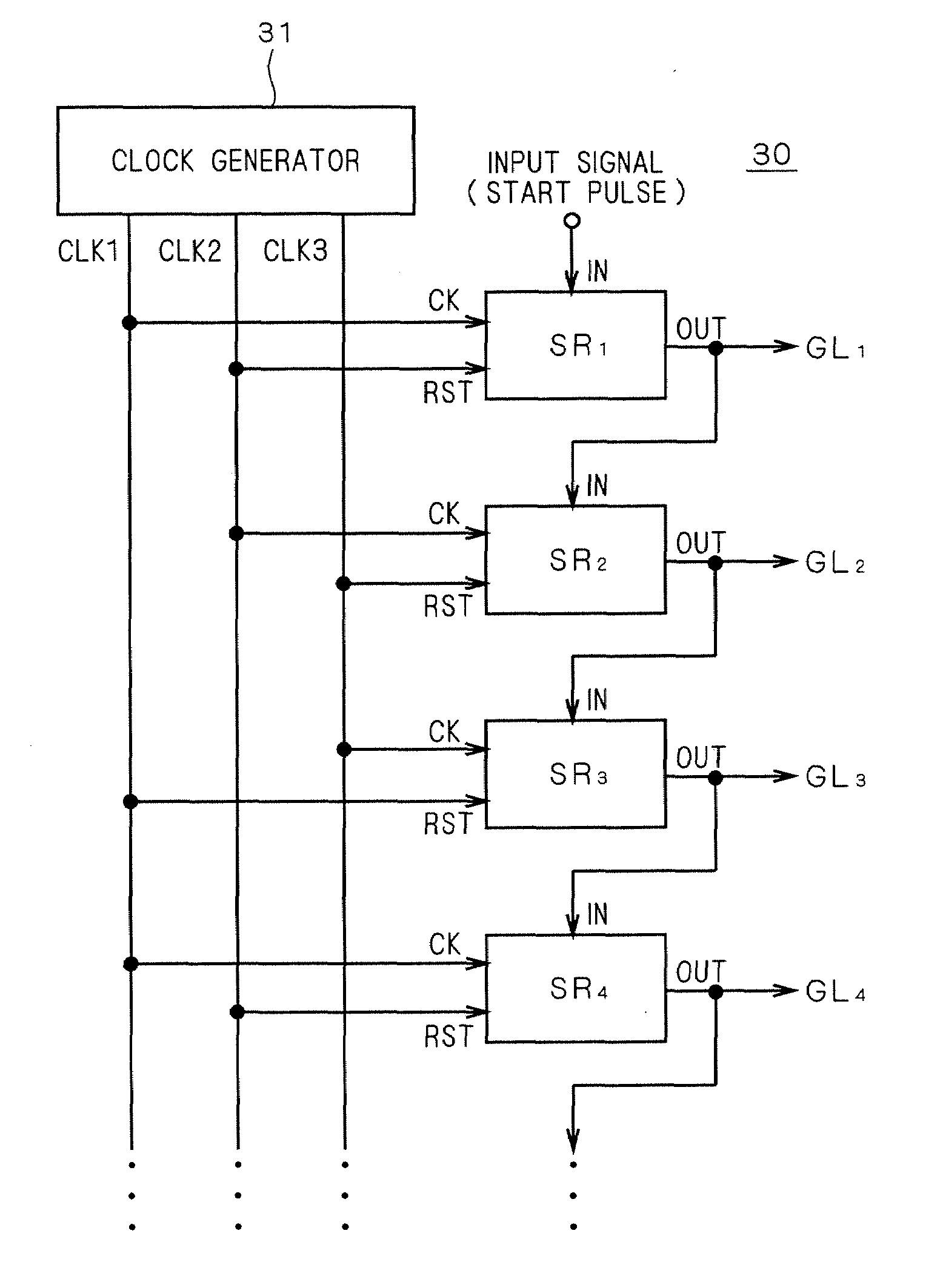
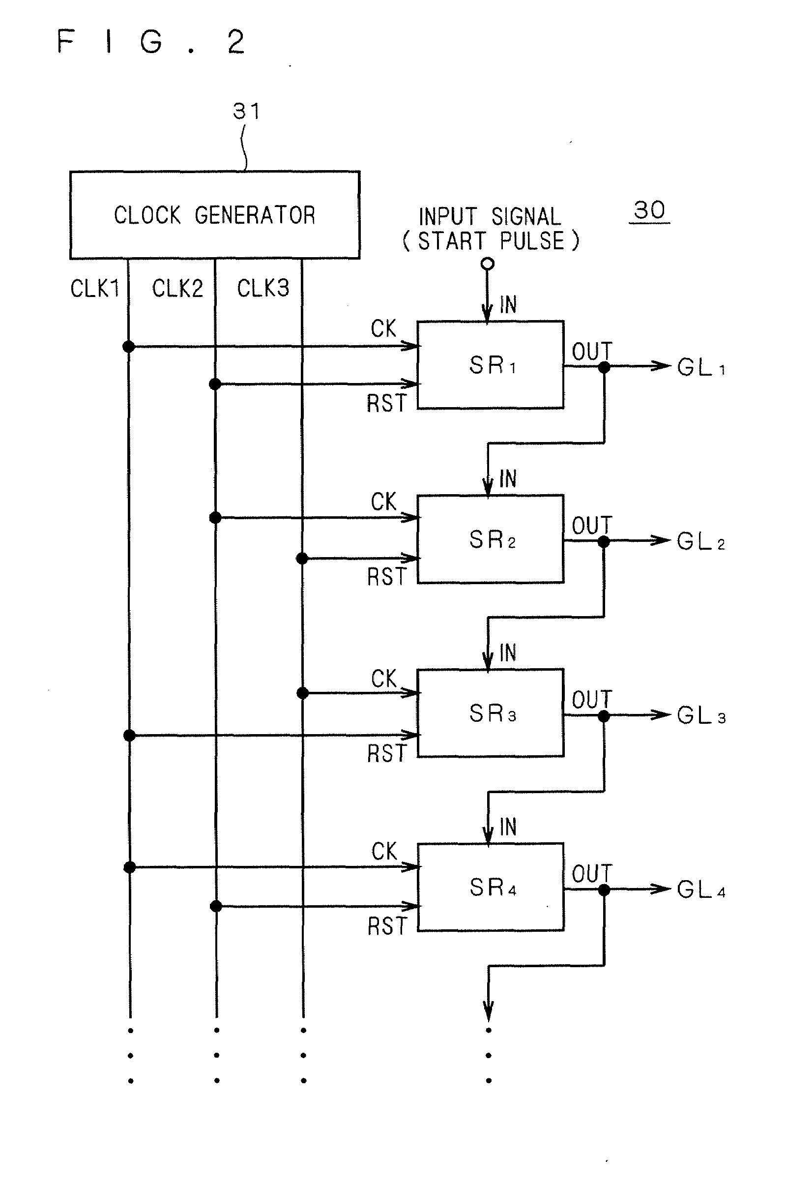
[0035]The liquid crystal display 10 is provided with a liquid crystal array part 20, a gate-line driving circuit (scanning-line driving circuit) 30 and a source driver 40. As will be described later explicitly, a shift register according to the present embodiment is mounted on the gate-line driving circuit 30.

[0036]The liquid crystal array part 20 includes a plurality of pixels 25 arrayed in a matrix. The columns of pixels (hereinafter also referred to as “pixel lines”) are respectively provided with gate lines GL1, GL2, . . . (hereinafter also generically referred to as a “gate line GL”), and the rows of pixels (hereinafter also referred to as “pixel rows”) are respectively provided with data lines DL1, DL2, . . . (hereinafter generic...

second preferred embodiment

[0109]In the unit shift register SR according to the first preferred embodiment, the transistor Q6A constituting the first inverter and the transistor Q6B constituting the second inverter are both diode-connected. In other words, the transistor Q6A has its gate and drain both connected to the first control terminal CTA to which the first control signal VFR is input, and the transistor Q6B has its gate and drain both connected to the second control terminal CTB to which the second control signal / VFR is input.

[0110]FIG. 10 is a circuit diagram illustrating the configuration of a unit shift register SR according to a second preferred embodiment. As shown in the drawing, the transistor Q6A has its gate connected to the first control terminal CTA, but its drain connected to the third power terminal S3 to which the high supply voltage VDD is input. Similarly, the transistor Q6B has its gate connected to the second control terminal CTB, but its drain connected to the third power terminal ...

third preferred embodiment

[0114]FIG. 11 is a circuit diagram illustrating the configuration of a unit shift register SR according to a third preferred embodiment. According to the present embodiment, the transistor Q3 has its drain connected to the input terminal IN, not to the power source. This can reduce the area occupied by a wire for power supply. However, it should be noted that the input terminal IN is connected to the output terminal OUT of the immediately preceding stage, which increases a load on the output stage of each unit shift register SR, so that the speed of circuit operation may be reduced.

[0115]While FIG. 11 shows an example of the present embodiment applied to the circuit according to the first preferred embodiment (FIG. 7), the present embodiment may also be applied to the circuit according to the second preferred embodiment (FIG. 10).


PUM


Abstract

A unit shift register includes first and second transistors for supplying low supply voltage to an output terminal. First and second control signals which are complementary to each other are input to first and second control terminals, respectively. A third transistor is connected between the first transistor and first control terminal, and a fourth transistor is connected between the second transistor and second control terminal. The third and fourth transistors each have its drain connected to the gate of each other in a crossed manner.

Description

BACKGROUND OF THE INVENTION[0001]1. Field of the Invention[0002]The present invention relates to a shift register, and more particularly, to a shift register for use as a scanning-line driving circuit for an image display apparatus or the like, which is formed of field effect transistors of the same conductivity type only.[0003]2. Description of the Background Art[0004]An image display apparatus (hereinafter referred to as a “display apparatus”) such as a liquid crystal display includes a display panel in which a plurality of pixels are arrayed in a matrix. A gate line (scanning line) is provided for each row of pixels (pixel line), and gate lines are sequentially selected and driven in a cycle of one horizontal period of a display signal, so that a displayed image is updated. As a gate-line driving circuit (scanning-line driving circuit) for sequentially selecting and driving pixel lines, i.e., gate lines, a shift register for performing a shift operation in one frame period of a d...

Claims


Application Information

Patent Timeline
IPC IPC(8): G11C19/00
CPCG11C19/28G09G3/20G09G3/36G11C19/00H03K19/00
Inventor TOBITA, YOUICHI
Owner TRIVALE TECH LLC
Why Eureka
Try Eureka