Leakage barrier for GaN based HEMT active device

a technology of active devices and leakage barriers, which is applied in the direction of basic electric elements, semiconductor devices, electrical equipment, etc., can solve the problems of poor electrical isolation between the source and gate, poor leakage current and inapplicability of gan based materials insulated gate techniques

Active Publication Date: 2007-09-20
NORTHROP GRUMMAN SYST CORP
View PDF15 Cites 5 Cited by
  • Summary
  • Abstract
  • Description
  • Claims
  • Application Information

AI Technical Summary

Problems solved by technology

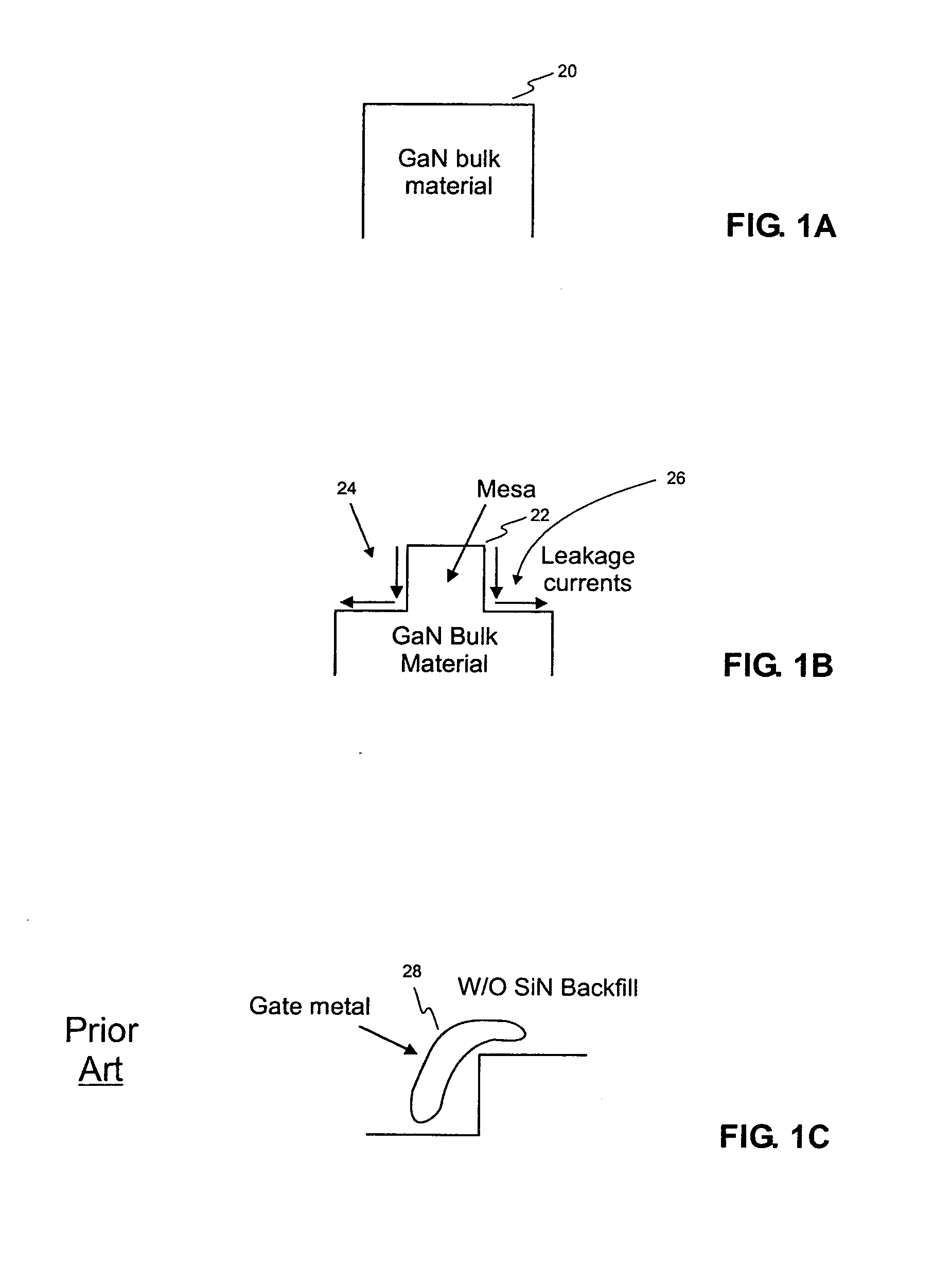
Such GaN based HEMT devices are known to have relatively high gate leakage current.
While the above technique may work fairly well with GaN/AlGaN HEMT layered devices, this technique is not applicable to HEMT devices formed without an insulated gate from GaN based materials.
As shown in FIG. 1B, these step discontinuities 24 and 26 allow undesirable leakage currents to flow ...

Method used


Image

  • Leakage barrier for GaN based HEMT active device
  • Leakage barrier for GaN based HEMT active device
  • Leakage barrier for GaN based HEMT active device

Examples


Embodiment Construction

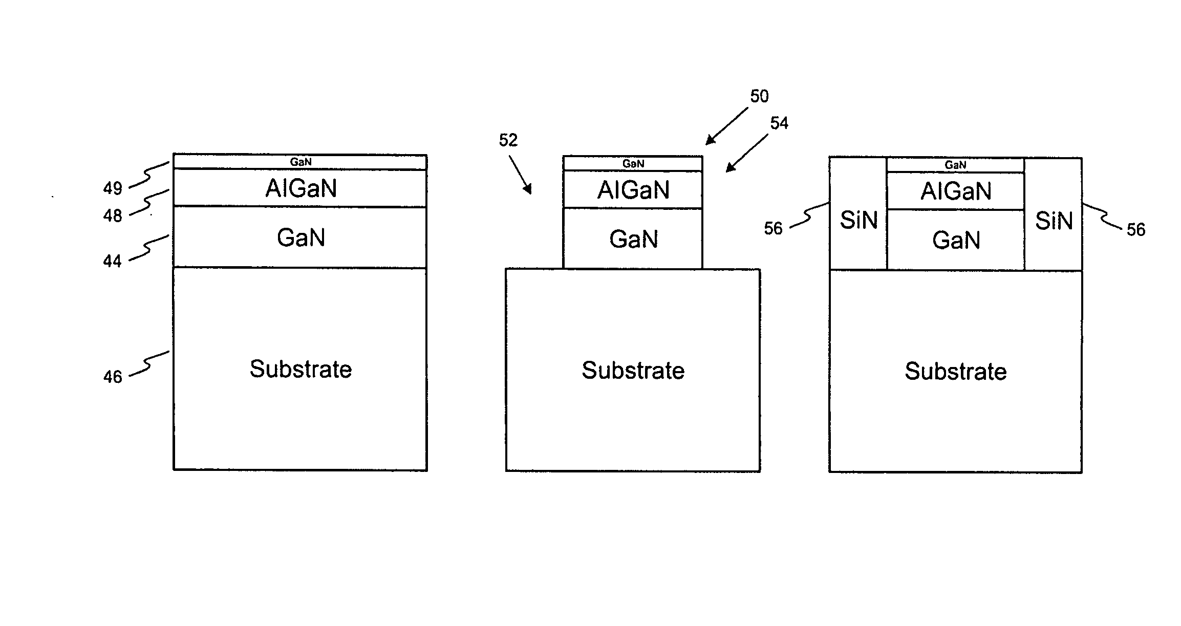
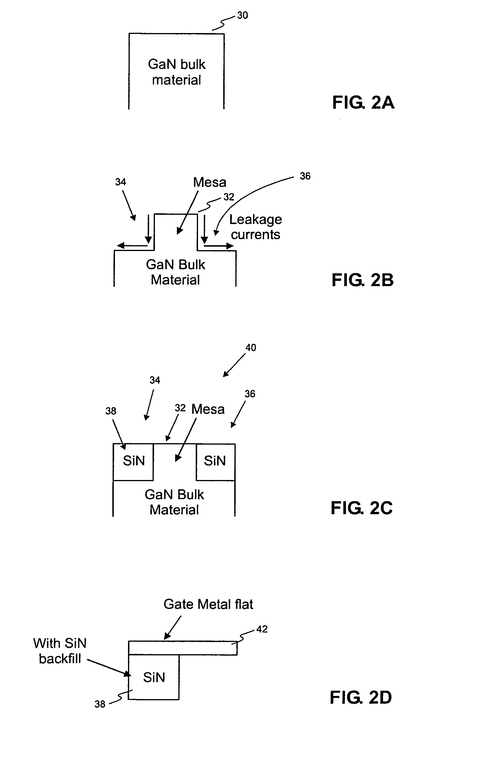
[0018] The present invention relates to a HEMT formed from a GaN material system which has relatively less leakage current than known HEMTs formed from GaN material systems and also solves the problem of current constriction of the gate metal. Two embodiments of the invention are disclosed. One embodiment, illustrated in FIGS. 2A-2D, relates to an embodiment of the invention in which the HEMT is formed from bulk GaN material. An alternate embodiment of the invention is illustrated in FIGS. 3A-3F in which the HEMT is formed from GaN / AlGaN.

[0019] Referring to FIGS. 2A-2D, a simplified explanation of the process in accordance with one embodiment of the present invention is provided. Referring first to FIG. 2A, a bulk GaN material 30 may be used as the starting point for the HEMT. The bulk GaN material is masked by convention photolithography techniques and etched, for example, by buffered oxide wet or Cl-based dry etching, to form a mesa 32. The gate mesa 32 defines a pair of step dis...


PUM


Abstract

An improved HEMT formed from a GaN material system is disclosed which has reduced gate leakage current relative to known GaN based HEMTs and eliminates the problem of current constrictions resulting from deposition of the gate metal over the step discontinuities formed over the gate mesa. The HEMT device is formed from a GaN material system. One or more GaN based materials are layered and etched to form a gate mesa with step discontinuities defining source and drain regions. In order to reduce the leakage current, the step discontinuities are back-filled with an insulating material, such as silicon nitride (SiN), forming a flat surface relative to the source and drain regions, to enable to the gate metal to lay flat. By back-filling the source and drain regions with an insulating material, leakage currents between the gate and source and the gate and drain are greatly reduced. In addition, current constrictions resulting from the deposition of the gate metal over a step discontinuity are virtually eliminated.

Description

BACKGROUND OF THE INVENTION [0001] 1. Technical Field [0002] The present invention relates to a high electron mobility transistor (HEMT) formed from a gallium nitride (GaN) material system and more particularly to GaN based HEMT transistor with reduced leakage current. [0003] 2. Description of the Prior Art [0004] High electron mobility transistors (HEMTs) are well known in the art and are known to be used are used in various low noise and power microwave applications where high device output power, power added efficiency and noise performance are critical. HEMTs are known to be used in Q, V and W band microwave power amplifiers in commercial and military radar systems, communications systems and the like. HEMTs are also known to be effectively integrated into monolithic microwave integrated circuits and monolithic millimeter wave integrated circuits (MMICs) including phased arrays for radiating at high power levels. [0005] HEMTs formed from Gallium Nitride (GaN) material systems ar...

Claims


Application Information

Patent Timeline
IPC IPC(8): H01L21/8234H01L21/336
CPCH01L29/2003H01L29/7783H01L29/66462
Inventor SANDHU, RAJINDER RANDYBARSKY, MICHAEL EDWARDWOJTOWICZ, MICHAEL
Owner NORTHROP GRUMMAN SYST CORP
Why Eureka
Try Eureka