Touch Panel And Protective Panel For Display Window Of Electronic Device Using The Same

a technology of electronic devices and protective panels, which is applied in the direction of electrical connection formation of printed elements, emergency connections, instruments, etc., can solve the problems of difficult to say that the electrodes themselves have high strength, conductor wires are broken at the connecting parts, and touch panels may need to be replaced with new ones, etc., to achieve stable contact resistance, easy mounting of touch panels and electrical connection of touch panels to interfaces, and easy operation. convenient and convenient

Inactive Publication Date: 2007-09-20
NISSHA PRINTING COMPANY
View PDF9 Cites 32 Cited by
  • Summary
  • Abstract
  • Description
  • Claims
  • Application Information

AI Technical Summary

Benefits of technology

[0028] In the present invention, the touch panel and the protective panel for a display window of an electronic device using the touch panel having such a structure described above produce the following effects.
[0029] Unlike the conventional touch panel requiring fitting accuracy of recessed (female) fittings or convex (male) fittings, the touch panel of the present invention does not require fitting accuracy because signals from the resistive films can be outputted to the outside through only contact at a planar area provided on the lower surface of the non-touch side substrate and provides a margin absorbing an error. As a result, mounting of the touch panel and electrical connection of the touch panel to an interface can be carried out more easily and very convenient compared to the conventional touch panel. Also, detachment of the touch panel and electrical disconnection of the touch panel from the interface can be easily carried out.
[0030] Further, unlike the conventional touch panel to be electrically connected to an interface by fitting using recessed (female) fittings or convex (male) fittings, the touch panel of the present invention is connected to an interface by contact at a planar area provided on the lower surface of the non-touch side substrate. Therefore, the touch panel of the present invention can be connected to an interface by pressing spring connector pins or the like provided in the interface against the flat electrodes for connection, which makes it possible to obtain stable contact resistance.

Problems solved by technology

However, the touch side substrate is formed from a resin sheet, the electrodes are formed of a silver paste, it is hard to say that the electrodes themselves have high strength.
Therefore, if a slightly large force is applied to the lead wire, there is a possibility that the conducting wire is broken at the connecting part.
Furthermore, when the touch panel is frequently touched by a sharp pen point, the touch panel may need to be replaced with new one due to the damage on the surface of the touch side substrate.
In this case, the maintenance by users becomes complicated.
More specifically, if the accuracy of position of the through-holes 4a, 4b, 4c, and 4d formed in the touch panel, the accuracy of inner diameter of the recessed (female) fittings 7, the accuracy of position of other convex (male) fittings, such as connector pins 12, provided in an interface so as to be fitted in the recessed (female) fittings 7, the accuracy of outer diameter of the other convex (male) fittings, or the accuracy of position of the touch panel mounted to a device is low, it will be difficult to fit the recessed (female) fittings 7 to other convex (male) fittings.
As a result, it is impossible to mount the touch panel on a device properly and to connect the touch panel to the interface electrically.
If the recessed (female) fittings 7 are forced to fit to other convex (male) fittings, stress is always applied to the touch panel, as a result, there is a possibility that the touch panel is deformed or cracked by an environmental resistance test (e.g., by temperature changes).
In addition, there are also a possibilities that the touch panel is cracked due to repetition of attachment and detachment thereof and stable contact resistance is impaired.
On the other hand, even in a case where the recessed (female) fittings 7 are smoothly fitted to other convex (male) fittings, when contact between the recessed (female) fittings 7 and other convex (male) fittings is poor, stable contact resistance cannot be obtained.

Method used


Image

  • Touch Panel And Protective Panel For Display Window Of Electronic Device Using The Same
  • Touch Panel And Protective Panel For Display Window Of Electronic Device Using The Same
  • Touch Panel And Protective Panel For Display Window Of Electronic Device Using The Same

Examples


first embodiment

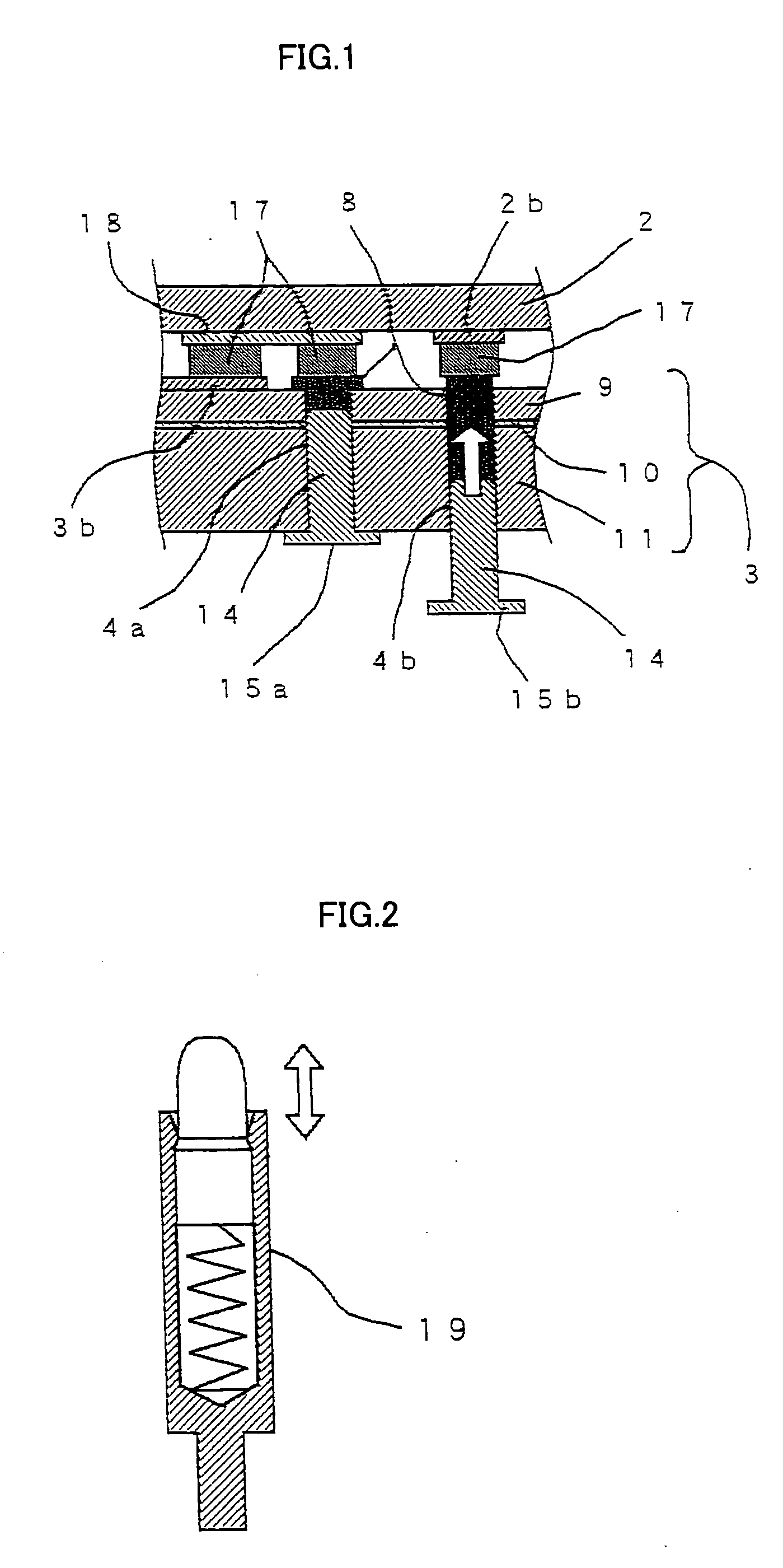
[0050]FIG. 1 illustrates a first embodiment of a touch panel according to the present invention.

[0051] It is noted that a method for assembling the touch panel of the present invention is the same as a conventional method shown in FIG. 11, and therefore a touch panel 1 will be first described with reference to FIG. 11.

[0052] As illustrated in FIG. 11, a resistive film 2a is formed by applying ITO or the like onto the lower surface of a touch side substrate 2 by way of sputtering or vacuum deposition. Also, on the upper surface of a non-touch side substrate 3, a rectangular resistive film 3a is formed in the same manner.

[0053] At the periphery of the non-touch side substrate 3, through-holes 4a, 4b, 4c, and 4d for constituting a connecting part 5 are formed to provide a touch panel in which an FPC (not shown in the drawing) is not directly drawn out from the side face thereof.

[0054] The touch panel 1 of the present invention having such a structure described above is characterize...

second embodiment

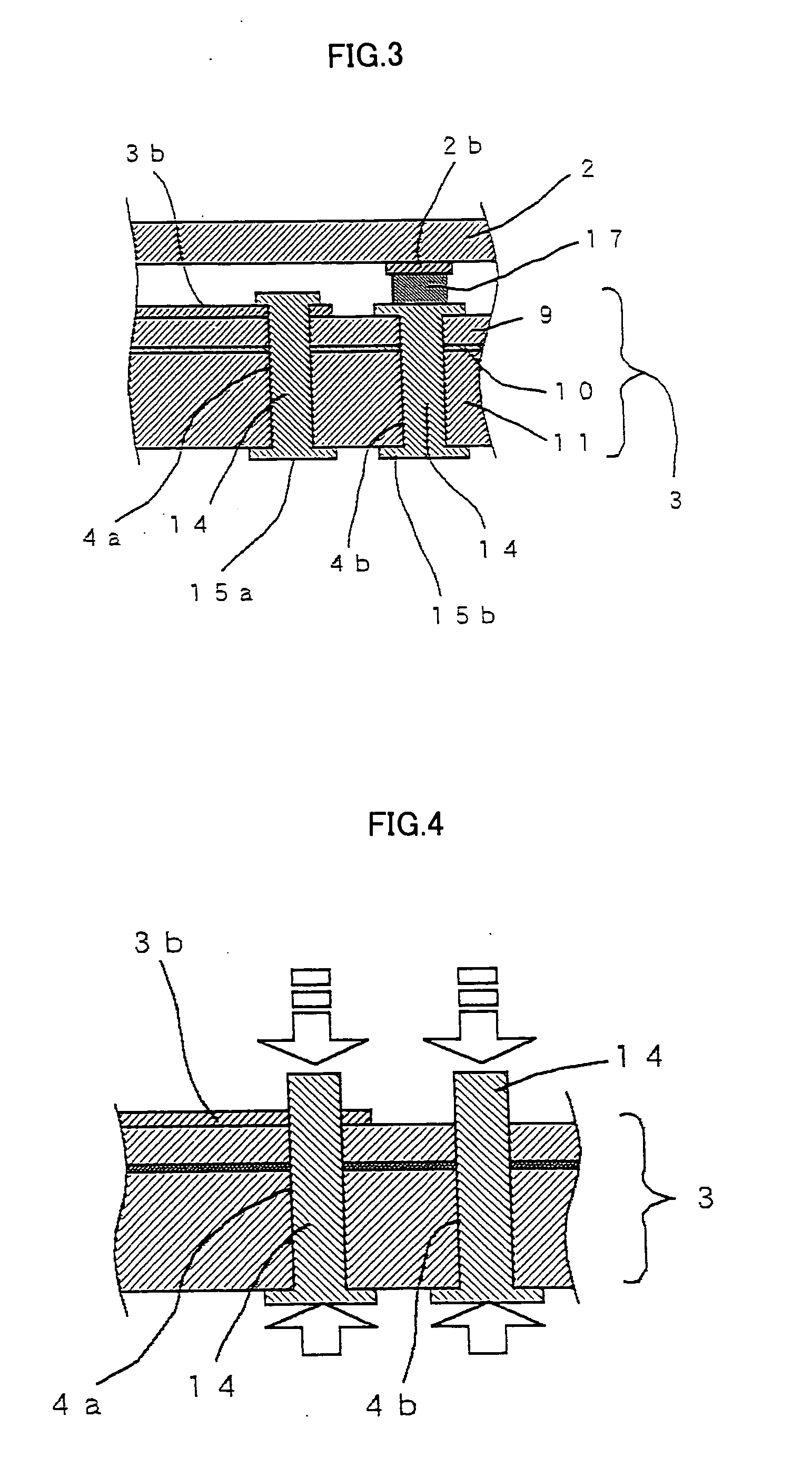
[0081]FIG. 3 illustrates a second embodiment of the touch panel according to the present invention.

[0082] The touch panel shown in FIG. 3 is characterized in that the rivet 14 provided in each of the through-holes 4a and 4b has heads at both ends of a shaft thereof. More specifically, after the rivet 14 having a head is inserted into each of the through-holes 4a and 4b for constituting the connecting part 5, the tip of a shaft of the rivet 14 also be formed into a head. One of the heads of the rivet 14 provided on the lower surface of the non-touch side substrate 3 forms the flat connecting electrode 15a or 15b for connection to an external terminal, and the other head of the rivet 14 is directly electrically connected to the electrode 2b or 3b of the resistive film 2a or 3a without through the communicating electrode 18. It is noted that the through-holes 4c and 4d are the same as the through-holes 4a and 4b, and are therefore omitted from FIG. 3.

[0083] The rivet 14 having heads ...

third embodiment

[0087]FIG. 6 illustrates a third embodiment of the touch panel according to the present invention.

[0088] The touch panel of the third embodiment shown in FIG. 6 is characterized in that a metal foil 16 is used instead of the rivet 14 to form a head. More specifically, the conductive paste 8 is injected into the through-holes 4a and 4b constituting the connecting part 5, and an opening of each of the through-holes 4a and 4b provided in the lower surface of the non-touch side substrate 3 and a periphery of the opening of the through hole are covered with a disk-like shaped metal foil 16. The metal foil 16 provided on the lower surface of the non-touch side substrate 3 forms the flat electrode 15a or 15b for connection to an external terminal. It is noted that the through-holes 4c and 4d are the same as the through-holes 4a and 4b, and are therefore omitted from FIG. 6.

[0089] Examples of a material for forming the metal foil 16 include copper, iron, nickel, and aluminum. The thicknes...


PUM

PropertyMeasurementUnit
thicknessaaaaaaaaaa
thicknessaaaaaaaaaa
diameteraaaaaaaaaa

Abstract

There is provided a touch panel capable of obtaining a stable connection resistance without requiring fitting accuracy at the time of the connection to an external terminal, and a protective panel for a display window of an electronic device using the same. The analog type touch panel includes a touch side substrate 2 and a non-touch side substrate 3 each having resistive films 2a, 3a provided on opposed inner surfaces thereof. Through-holes 4a, 4b, 4c, 4d formed at the periphery of the non-touch side substrate 3. A connecting part 5 for electrically connecting electrodes of the resistive films 2a, 3a to an external terminal, in which a conductive paste is injected into the through-holes and a rivet 14 is inserted into each of the through-holes from the lower surface side so that a head of the rivet 14 forms flat connecting electrodes 15a, 15b for connection to the external terminal on the lower surface of the non-touch side substrate 3.

Description

TECHNICAL FIELD [0001] The present invention relates to a touch panel to be used as a coordinate input means and a touch position detecting means and a protective panel for a display window of an electronic device using the same. BACKGROUND ART [0002] A touch panel includes two substrates opposed to each other and resistive films provided on opposed inner surfaces of the substrates. Further, on both ends of each of the resistive films, there are provided electrodes. Such a touch panel operates on principles that power is externally supplied to both the resistive films alternately and an electrical signal corresponding to a position where the two resistive films are brought into contact with each other by a touch event is outputted to the outside via the electrodes to which no power is supplied. Usually, in view of the output of signals to the outside, each of the electrodes extends to a position corresponding to the position of a connecting part of the touch panel, and the ends of t...

Claims


Application Information

Patent Timeline
Patent Type & Authority Applications(United States)
IPC IPC(8): H04M1/00G06F3/048H01H9/02H01H13/70H01H13/785H05K3/40
CPCG06F3/045H01H13/785H01H2201/036H01H2207/00H05K2201/10416H05K3/4046H05K3/4069H05K2201/09909H05K1/116G06F3/04164
Inventor NISHIKAWA, KAZUHIROKAI, YOSHIHIRONAKAMURA, KAZUTO
Owner NISSHA PRINTING COMPANY
Why Eureka
Try Eureka